COMMISSION D: Electronics and Photonics
(November 2007 - October 2010)
Edited
by Tadao Nagatsuma
Electronics and Photonics cover huge scientific and technological fields. Among them, in this report, we have selected several important topical areas, where in particular Japanese leading researchers have actively contributed between 2007 and 2010. They overviewed recent remarkable advances in their specialized areas.
The following is a list of areas that the chapter editor has taken up.
D1. Metamaterials
E. Sano
Hokkaido University
D2. Quantum Cascade Lasers
K. Kasahara
Ritsumeikan University
D3. Applications of THz Quantum Cascade Lasers
I. Hosako
National Institute of Information and Communications Technology
D4. Nonlinear Optical Waveguide for THz Tomography
K. Kawase
Nagaya University
D5. Photonic Millimeter-Wave Technology
H. Ito
Kitasato University
D6. Plasmonic Device Technology for Emission and Detection
of THz Radiation
T. Otsuji
Tohoku University
D7. Integrated Josephson Voltage Standard Technology
S. Kohjiro
National Institute of Advanced Industrial Science and Technology
D8. High Capacity Optical Fiber Transmission Systems
H. Toda
Doshisha University
D9. Radio-on-Fiber Technologies for Heterogeneous Wireless Services
K. Tsukamoto
Osaka University
D10. Broadband Access Networks with Wired and Wireless
Integration/Convergence
K. Iwatsuki
NTT
D11. Body Area Network
Y. Kado
Kyoto Institute of Technology
D1. Metamaterials
Eiichi Sano
Hokkaido University
Recently, there has been significant interest in researching and developing wireless communication circuits for 3.1-10.6 GHz ultra-wideband, 24-GHz band, and 60-GHz band applications. Modern CMOS technologies enable high-level integration of RF, physical layer (PHY), and medium access control (MAC) layer processors, thus reducing the size and cost of wireless equipment. In recent years, several extensive attempts have been made to fabricate antennas on Si substrates for inter-chip or intra-chip transmissions. However, a high-resistivity float zone (FZ) and proton-bombarded Si substrate of more than 5 kΩcm have been used to fabricate high-gain antennas. This is because the low-resistivity Si substrates commonly used in CMOS processes degrade the antenna gain. When standard 10-Ωcm substrates are used, transmission gains range from -50 to -60 dB for transmissions over a few centimeters. Thus, an ingenious development is needed to increase the gains of antennas fabricated on low-resistivity Si substrates.
An artificial dielectric layer (ADL) produces an extremely high permittivity.
An ADL has been developed to shield coplanar waveguides (CPWs) from Si substrate.
Figure 1 shows a schematic of the ADL. Two identical metal patch arrays are formed on the two metal layers.
One patch array is shifted by one-half cell pitch to the other patch array. An insulating layer with a dielectric constant εd
and a thickness td is sandwiched between the two metal layers. The dielectric constant along the surface of the ADL is given by

where A is a quarter the area of a square metal patch and t is the total thickness of the ADL.
Å@
As found in Eq. 1, ε// is increased by decreasing the layer thickness t and td and/or by increasing the patch area. Fig.ure 2 shows potential distributions demonstrating the shielding effect of ADL. The CPWs with and without ADLs were simulated with a finite-difference time-domain (FDTD) electromagnetic simulator. The ADL was modeled as a uniform sheet with &epsilon// of 104. The signal source was sine waves of 10 GHz. As shown in Fig. 2, the electric field was terminated in the ADL. When an electromagnetic wave illuminates an ADL with high ε// placed above a Si substrate, the electric field strength in the Si substrate reduces more than when no ADL is on the Si substrate. Placing an ADL between the antenna and Si substrate is expected to increases the antenna gain.
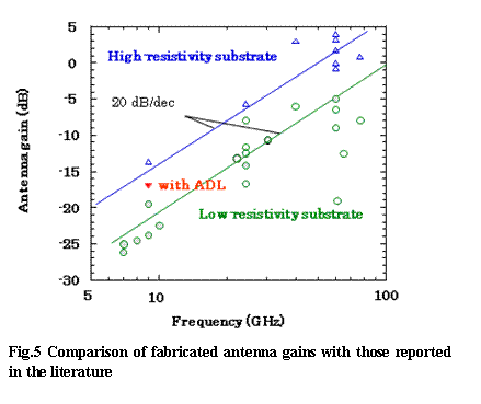
Three kinds of antennas were designed and fabricated: an antenna with ADL shielding, an antenna without ADL fabricated on a low-resistivity (Å`10 Ωcm) Si substrate, and an antenna without ADL fabricated on a high-resistivity (>1 kΩcm) Si substrate. Figure 3 is a microphotograph of fabricated antenna with the ADL. Figure 4 shows the measured and simulated antenna gains. At 9 GHz, the ADL improved the antenna gain by 3-dB more than the antenna on the low-resistivity Si substrate. This is the higher gain ever archived for the antennas fabricated on a low-resistivity Si substrate operating at around 9 GHz. Figure 5 compares the antenna gains achieved in this work with those reported in previous literature. Further improvement will be possible by reducing the dielectric layer thickness to increase dielectric constant and reducing the loss of poly-Si layer.
References
[2]K. Takahagi and E. Sano, ÅgHigh-gain silicon on-chip antenna with artificial dielectric layer,Åh Proc. 2010 Asia-Pacific Radio Science Conf., paper DC1-5, 2010.
[3]M. Ikebe, D. Ueo, K. Takahagi, M. Ohuno, Y. Takada, and E. Sano,ÅgA3.1-10.6 GHz RF CMOS circuits monolithically integrated with dipole antenna,Åh Proc. 2009 IEEE Int'l Conf. Electronics Circuits and Systems, pp.17-20, 2009.
[4]K. Takahagi, M. Ohno, M. Ikebe, and E. Sano,ÅgUltra-wideband silicon on-chip antennas with artificial dielectric layerÅh, Proc. 2009 Int'l Sympo. Intelligent Signal Processing and Communication Systems, pp. 81-84, 2009.
D2. Quantum Cascade Lasers
K. Kasahara
Ritsumeikan University
Since they first appeared, the operation frequency of quantum cascade lasers (QCLs) has been extended from the mid-infrared to the far-infrared range, and QCLs have become the most desirable tool for such applications as trace gas analysis owing to the continuous tunability of their emission range. The progress of QCLs has been achieved by focusing on the active region designs that make full use of wave function engineering. A continuous wave (cw) operation up to above 60 ÅãC has been reported for 7.9 µm InGaAs/InAlAs QCLs with single phonon resonance-continuum (SPC) depopulation, exhibiting a threshold current density of 2.23 kA/cm2 and emitting a cw output power of 36 mW at 30 ÅãC [1, 2]. In the SPC depopulation structure, the lower lasing state of the active region is designed to be separated by one phonon energy from the top state of the miniband, enabling fast electron depopulation from the lower lasing state and subsequent fast electron extraction. This structure can alleviate the problem caused by fluctuations of the energy separation between the lower states, which is usually observed with a single phonon depopulation three quantum well-used design, leading to a successful commercial mass production of QCLs.
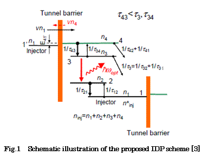
High stability for temperature changes has been demonstrated with 8 É m QCLs introducing the indirect pump (IDP) [3]. Threshold current densities were 2.7 and 3.3 kA/cm2 for cavity lengths of 4 and 1.5 mm, respectively. Respective characteristic temperatures T0 were as high as 243 and 303 K around room temperature. Maximum output powers were 362 and 50 mW. T0-value of 303 K was the highest record ever reported with QCLs. In the IDP, electrons are injected into the intermediate state, level 4 via electron tunneling from the ground state, level 1Åf in the previous injector and then, are relaxed quickly down to the upper laser state, level 3 by LO-phonon emissions (Fig. 1). In this circumstance, the electron population n4 at level 4 is expected to be low, and the backward tunneling current ( n4) is kept to be lower than the forward tunneling current ( n1) even when the electron population n3 at level 3 approaches a high value comparable to the injector doping density. High device performance of InGaAs/InAlAs Fabry-Perot QCLs based on the indirect pump scheme was also demonstrated at 15 µm [4]. A low threshold-current-density of 3.5 kA/cm2, a high maximum output power of 216 mW, and a high slope efficiency of 346 mW/A, were obtained all at room temperature. The observed extremely high T0 of 450 K over wide temperature range, 320-380 K was ascribed to a strong suppression of electron populations in injectors.
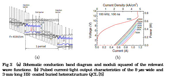
To generate new opportunities for broad gain band applications, homogeneous broad-gain QCLs based on dual-upper-state design have been demonstrated at 8.4 µm [5]. The devices exhibited a homogeneously wide electroluminescence spectrum of 330 cm-1 of which shapes were insensitive to voltage changes as well as extremely high temperature insensitivity of the laser. The strongly coupled two upper laser states and the lower laser state were associated with the wave functions [Fig. 2 (a)]. The electron populations in the both upper laser states were kept to be equal, because of the small energy gap between the two upper states of 20 meV. The QCLs had a homogeneously broadened gain spectrum due not only to the appropriate energy difference between the two states but also to equal oscillator strengths of the transitions from the both upper laser states to the lower common laser state. A buried heterostructure was used in them, and a high cw output power of 152 mW together with a high constant slope efficiency of 518 W/A at room temperature was obtained. In addition, the device performance was insensitive to temperature change; T0-values of 306 K and constant slope efficiency over the wide temperature range, 280-400 K [Fig. 2 (b)].
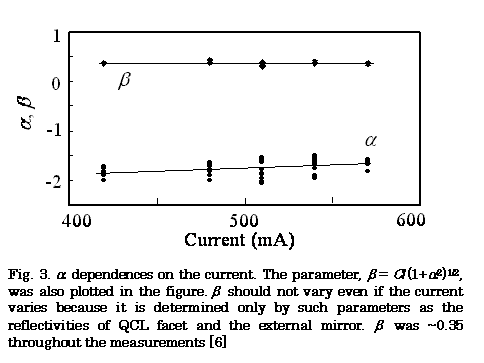
The linewidths of QCLs are broadened by the α-factor, as is the case of conventional semiconductor laser diodes (LDs). Typical values for interband-using LDs lie in the range α= 2-7. By contrast, it had been predicted that QCLs would have an αof zero as a result of intersubband symmetric gains. However, deviation from zero is possible. The α-factor is closely connected to the QCL gain profile and provides information on the shape of the gain. Investigating the QCLÅfs α-factor, therefore, is of considerable importance, offering clues about the physical parameters relevant to the gain, such as the electron distribution in the subbands. Until now, however, only a limited number of experimental studies on the α-factor of the QCL have been undertaken, particularly as to its current dependence. The α-factor of a commercially available 6.1 µm InGaAs/InAlAs QCLs with an SPC structure capable of cw operation with a Peltier cooler, and its current dependence were investigated in detail [6]. The αwas tended to increase slowly with an increase in current, and was in the range of -1.8 to -1.7 (Fig. 3). The α probably affected by detuning, was still smaller than that of the conventional 1.55 µm semiconductor LDs.
Terahertz (THz) QCLs areÅ@expected to find applications in such areas as bio-sensingÅ@andÅ@security in addition to environmental monitoring. To date, the highestÅ@recorded operating temperatures for THz QCLs are 178 KÅ@in pulsed mode and 117 K in cw mode.Å@To aim at the achievement of THz QCLs operating at higher temperatures, four-level system used QCLs has been proposed [7]. It wasÅ@found that both a lower threshold current and higher slopeÅ@efficiency can be realized in the four-level system compared with the conventional three-level system. Furthermore,Å@it was found that the four-level system has aÅ@higher operating temperature tolerance than does the three levelÅ@system. These results are expected to lead to the developmentÅ@of THz QCLs that can be operated at high temperatures.
[2]K. Fujita, S. Furuta, A. Sugiyama, T. Ochiai, T. Edamura, N. Akikusa, M. Yamanishi, and H. Kan, ÅgHigh-Performance λÅ`8.6 µm quantum cascade lasers with single phonon-continuum depopulation structuresÅh,IEEE J. Quantum Electron., Vol.46, pp.683-688(2010).
[3]M. Yamanishi, K. Fujita, T. Edamura, and H. Kan,ÅgIndirect pump scheme for quantum cascade lasers: dynamics of electron-transport and very high T0-valuesÅh, Opt. Express, Vol. 16, pp.20748-20758 (2008).
[4]K. Fujita, M. Yamanishi, T. Edamura, A. Sugiyama, and S. Furuta, ÅgExtremely high T0-values (Å`450 K) of long-wavelength (Å`15 µm), low-threshold-current-density quantum-cascade lasers based on the indirect pump schemeÅh, Appl. Phys. Lett., Vol.97, 201109 (2010).
[5]K. Fujita, T. Edamura, S. Furuta, and M. Yamanishi,ÅgHigh-performance, homogeneous broad-gain quantum cascade lasers based on dual-upper-state designÅh,Appl. Phys. Lett., Vol.96, 241107(2010).
[6]M. Ishihara, T. Morimoto, S. Furuta, K. Kasahara, N. Akikusa, K. Fujita and T. Edamura,ÅgLinewidth Enhancement Factor of Quantum Cascade Lasers with a Single Phonon Resonance-Continuum Depopulation Structure on a Peltier CoolerÅh, Electron. Lett., Vol. 45, pp. 1168-1169 (2009).
[7]N. Sekine and I. Hosako,ÅgDesign and analysis of high-performance terahertz quantum cascade lasersÅh, Phys. Status Solidi C 6, pp. 1428-1431 (2009).
D3. Applications of THz Quantum Cascade Lasers
I. Hosako
National Institute of Information and Communications Technology
Since the terahertz quantum cascade laser (THz-QCL) has firstly demonstrated [1], many people have been investigated and improved its performances. And some had demonstrated imaging (THz-QCL as an illuminator) [2], local oscillator (for precision spectral sensing purpose) [3] and even wireless communication [4] using the THz-QCL. In those demonstrations, almost THz-QCLs were operated in cryogenic temperature conditions below 77K (Liquid nitrogen temperature) to achieve sufficient output power. For a cooling down to below 77K, liquid helium or large mechanical coolers must be required. And those cooling equipments are usually bulky and expensive. The requirements of those cooling equipments limit a practicality of the THz-QCL, even though lots of kinds of demonstration experiments have so far conducted.
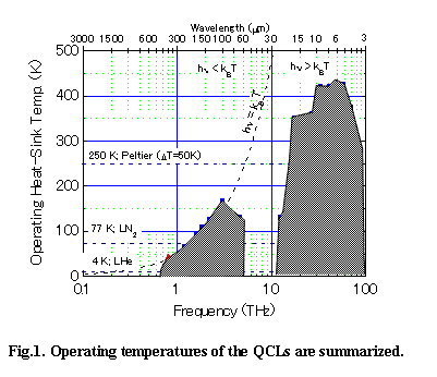
The recorded operating temperatures of the QCL (THz-QCLs and Mid IR-QCLs) are summarized in Figure 1. In the THz-frequency range, GaAs/AlGaAs-material system is mainly used for the QCL. On the other hand, InGaAs/InAlAs/InP-material system is mainly used for the Mid-IR QCLs. The frequency gap between 5 THz and 10 THz is caused by strong phonon absorption of GaAs/AlGaAs or InGaAs/InAlAs/InP-material systems. The highest operating temperature of the THz-QCL was recorded as 186K at 3THz based on a resonant LO-phonon type active structure and a double-metal waveguide structure [5]. The room temperature (even in the thermoelectric cooling temperature) operation of the THz-QCLs has not yet achieved, even though there is no theoretical limitations. At this moment, the most practical way to cool down the THz-QCL is to use the liquid nitrogen for ÅgrealÅh applications.
NEC Guidance and Electro-Optics Division and National Institute of Information and Communications Technology (NICT) have developed a real-time terahertz imaging system consisting of the liquid nitrogen cooled THz-QCL illuminator and uncooled microbolometer array detector[7]. As applications of the their real-time terahertz imaging system, a stand-off imaging system that could be useful in a fire disaster relief and a label-free bio-materials detection system have developed and demonstrated.
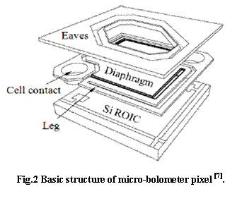
Liquid nitrogen cooled compact THz-QCL system has been developed for the external light source. By that system, the average output of a few micro watts can be obtained at 3.1 THz. The emission power is large enough for the improved un-cooled micro-bolometer array (320 x 240 elements). The THz-QCL consists of the super-lattice structure of GaAs/AlGaAs, and the structure of one active unit is almost same as the one written in the literature [6-8]. The active layer consists of all 480 active units, and its thickness is about 25 É m. The resonator is 200-É m-wide single metal type waveguide, and length is 3 mm [7, 8]. A micro-bolometer array has the structure shown in Figure 2. By performing various kinds of improvement shown below, the improvement in sensitivity of about 2 orders magnitude was attained from the state before improvement [9]. The improvements were as follows. (1) The index of absorption of terahertz waves has been raised by tuning up the sheet resistance of the absorption film added by the addition. (2) The arm that provides the thermal conduction of the bolometer has been extended as an improvement of the thermal isolation structure. (3) The sensor package window material was made from high resistance silicon with a small absorption of the terahertz waves, and the anti-reflection coating by parylene was given to both sides. By those improvements, the noise equivalent power achieves about 8 times improvement from 250pW to 31pW in comparison with before improvement [9]. As well as the improvement of the micro-bolometer array sensor, optimizations of terahertz optics (a lens system and filters) are important for a real-time imaging system. A Fresnel lens with anti-reflection coat using high resistance silicone was created, and a metal mesh filter was used as a band path filter. The role of the filter is to prevent the emission of the 10-É m-band to be emitted from the objects at room temperature. Although radiation of the 10-É m-band from the filter has always reached the sensor, since it hardly changes, the signal of the portion can be excludable with processing in a sensor read-out circuit.
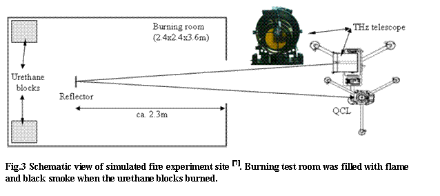
A stand-off (ca. 5 m in distance) terahertz imaging experiments were carried out under simulated fire conditions (See Figure 3). Under the fire conditions which generated hot and black smoke, terahertz images were obtained, while the smoke blocked visible light and saturated signal in long wavelength infrared (LWIR) region. The experimental results show advantage of terahertz over LWIR or visible. A video of the experiments will soon appear in NICT channel in YouTube [10].
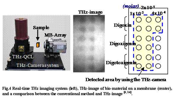
It is thought that biopolymers, such as protein and sugar protein, acted mutually considering very weak interactions, such as a hydrogen bond and van der Waals forces, as mediation, changed the combined state by the thermal energy about room temperature, and have developed its function. The energy of the terahertz wave is comparable as those weak couplings. Therefore, using terahertz radiation, without the use of labeling, it is expected that the knowledge about a difference, folding, etc. of the structure of biopolymers are acquired. So, one of promising application of the terahertz camera would be a label-free detection for a reaction of small molecules with proteins. It is possible to detect a small change in the amount of bio-material by using terahertz transmissive imaging, because very small amount of bio-material causes a large absorption of the terahertz waves. The terahertz wave penetrated the porous PVDF sheets (membrane) and, using the living body materials such as an antigen / the antibody strongly absorbing the terahertz wave, Ogawa et al. had developed a method to detect bio-materials without using chemical labels [11]. By using the terahertz camera, a label-free detection experiment of small molecule / protein reaction (Biotin [C10H16N2O3S, Molecular weight ca. 240] /Streptavidin [Molecular weight ca. 60,000]) were carried out only by placing the membrane to which bio-material adhered between the light source and sensor as shown in Figure 4 in collaboration with Prof. Y. Ogawa of Kyoto University [12]. In the experiments, detection sensitivity limit of the reaction was almost same as those of the conventional methods. In the figure, comparison with the method using the conventional label is performed. The terahertz images also have similar areas of the conventional label method. By the method described here, the images can be retrieved in real time immediately after the antigen-antibody reaction. It means that, since the work which attaches an indispensable label becomes unnecessary in the conventional label method, the throughput of whole work can be improved. Moreover, by that method, the development of the label set by each purpose itself becomes unnecessary. Therefore, a result can be obtained, without waiting for development of a label. Furthermore, this method is applicable also to the biopolymer of a small molecular weight. Since it is difficult to develop a label to the biopolymer of a small molecular weight, this terahertz-method is useful. Therefore, it can expect extensive application in fields, such as biotechnology, medical treatment, and agriculture. The advantage of label-free detection method by using the terahertz camera would be its throughput and low cost.
The real-time terahertz imaging system still has a large room to improve its performance. The sensitivity of the un-cooled micro-bolometer array system could be improved by one order of magnitude by optimizing the bolometer structure to the terahertz waves and improving bolometer material. In light source, a milliwatt class output of the THz-QCL can be expected in near future. In total, a figure of merit of the real-time terahertz imaging system can be expected to improve by 2 or 3 orders of magnitude.
[2]S. Kumar and A. Lee, ÅhResonant-Phonon Terahertz Quantum-Cascade Lasers and Video-Rate Terahertz Imaging,Åh IEEE Journal of Selected Topics in Quantum Electronics, Vol. 14, Issue 2 (2008) 333.
[3]D. Rabanus, U. U. Graf, M. Philipp, O. Ricken, J. Stutzki, B. Vowinkel, M. C.Wiedner, C. Walther, M. Fischer, and J. Faist, ÅgPhase locking of a 1.5 Terahertz quantum cascade laser and use as a local oscillator in a heterodyne HEB receiverÅh, OPTICS EXPRESS Vol. 17, No. 3 (2009) 1159.
[4]P. Grant, S. Laframboise, R. Dudek, M. Graf, A. Bezinger, H. Liu, ÅgTerahertz free space communications demonstration with quantum cascade laser and quantum well photodetector,Åh ELECTRONICS LETTERS, Vol. 45, Issue 18 (2009) 952.
[5]S Kumar, Q. Hu, and J. Reno,Åh 186 K operation of terahertz quantum-cascade lasers based on a diagonal design,Åh Appl. Phys. Lett., Vol. 94 (2009) 131105.
[6]B. S. Williams, S. Kumar, H. Callebaut, and Q. Hu, ÅgTerahertz quantum-cascade laser operating up to 137 KÅh, Appl. Phys. Lett., Vol. 83, No. 25, pp. 5142-5144 (2003).
[7]N. Sekine and I. Hosako, ÅgDesign and analysis of high-performance terahertz quantum cascade lasersÅh, Physica Status Solidi (c), Vol. 6, pp. 1428-1431 (2009).
[8]I. Hosako, N. Sekine, M. Patrashin, S. Saito, K. Fukunaga, Y. Kasai, P. Baron, T. Seta, J. Mendrok, S. Ochiai, and H. Yasuda, ÅgAt the Dawn of a New Era in Terahertz Technology,Åh Proceedings of the IEEE, Vol. 95, No. 8, pp.1611-1623 (2007).
[9]N. Oda, H. Yoneyama, T. Sasaki, M. Sano, S. Kurashina, I. Hosako, N. Sekine, T. Sudou, and T. Irie,ÅgDetection of terahertz radiation from quantum cascade laser using vanadium oxide microbolometer focal plane arraysÅh, Proc. SPIE, 6940, 69402Y-1-69402Y-12 (2008).
[10]http://www.youtube.com/user/nictchannel
[11]Y. Ogawa, S. Hayashi, M. Oikawa, C. Otani and K. Kawase, ÅgInterference terahertz label-free imaging for protein detection on a membrane,Åh Optics Express, Vol. 16, No. 26, pp.22083 - 22089 (2008).
[12]N. Oda, ÅgUncooled bolometer-type Terahertz focal plane array and camera for real-time imagingÅh, Comptes Rendus Physique, Vol.11, pp.496-509 (2010).
D4. Nonlinear Optical Waveguide for THz Tomography
K. Kawase
Nagaya University
Abstract-Nonlinear optical terahertz wave generation is a promising method for realizing a practical source with wide frequency range and high peak power. Unfortunately, many nonlinear crystals have strong absorption in the terahertz frequency region. This limits efficient and widely tunable terahertz wave generation. The Cherenkov phase-matching method is one of the most promising techniques for overcoming these problems. We propose a prism-coupled Cherenkov phase-matching method, in which a prism with a suitable refractive index at terahertz frequencies is coupled to a nonlinear crystal. We demonstrate prism-coupled Cherenkov phase-matching terahertz generation using the DAST and LiNbO3 crystals. With DAST crystal, we obtain a spectral flat tunability up to 10 THz by difference frequency generation. With LiNbO3 crystal, we observe a spectral flat broadband terahertz pulse generation up to 5 THz pumped by a femto second fiber laser. The obtained temporal waveform is an ideal half cycle pulse suitable for reflection terahertz tomography.
1. Cherenkov phase matching with prism coupler
Cherenkov THz radiation is generated inside a nonlinear crystal when the velocity of the polarization excited by a DFG process is greater than the phase velocity of the radiated wave. In general, many nonlinear crystals have strong dispersion between the optical and THz regions, and the refractive index at THz frequencies is larger than that at optical frequencies. This may result in behavior that satisfies the Cherenkov-type phase matching condition, i.e.
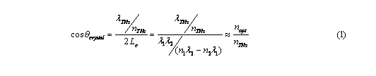
Where λ1 and λ2 are the wavelengths of the two signals contributing to the DFG process
(ω1 - ω2 = ωTHz), n1 and n2 (n1 = n2 ≈ n) are the refractive indices of the crystal at the pump wavelengths, and Lc is the coherence length of the surface-emitted process (Lc = ÉŒ/áôk, where áôk = k1 - k2 and k is the wave vector). The Cherenkov angle, θcrystal, is determined by the refractive index at the pump frequencies and that at the THz frequency in the crystal, and so the angle is strongly dependent on the nonlinear material. The emitted THz radiation propagates with the Cherenkov angle to the crystal-air interface, and if the angle is greater than a critical angle, which is determined by the difference in the refractive index at the interface, the THz wave undergoes total internal reflection at the interface. In order to prevent this, we use a cladding material with a suitable refractive index formed into a prism. The angle of the cladding-nonlinear crystal interface, θclad, is important for practical applications and can be determined using SnellÅfs law, as follows.
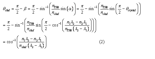
where nclad is the refractive index of the cladding layer in the THz-frequency range. This equation is equivalent to a model in which the THz wave radiates directly into the cladding layer. It indicates that nclad should be larger than that of the nonlinear crystal at the pump frequency, and also that it is not necessary to take into account the refractive index of the crystal at the THz frequency (as the equation does not depend on nTHz). We call the method as Prism Coupled Cherenkov Phase Matching (PCC-PM). For the PCC-PM THz-wave generation, by comparing the refractive index of the crystal at optical frequencies to that of Si (which is approximately 3.4 across the whole of the THz-frequency region), we see that Si is suitable as a Cherenkov radiation output coupler for many nonlinear crystals.
The organic nonlinear crystal DAST is attractive material for THz generation [1] because the crystal has a very large nonlinear coefficient. DAST is also strongly absorbing in the THz region, which has so far prevented efficient THz generation. The PCC-PC method, however, allows efficient THz generation with very high nonlinear efficiency. DAST has very similar refractive indices in the near infrared and THz-frequency regions, and this means that collinear phase matching can be achieved.
2. Widely tunable THz generation using DAST crystal
We performed an experiment to prove which is dominant for PCC-PM, Eq. 1 or 2. The 100-µm-thick DAST single crystal used was hexagonal so that we could achieve b-axis propagation of two pump beams. A Si prism was coupled along the (001) plane of the DAST crystal because as-grown DAST has a very flat surface in the plane. A dual-wavelength potassium titanium oxide phosphate (KTP) optical parametric oscillator (OPO) with pulse duration of 15 ns, pulse energy of 1.5 mJ, and 1300 -1600-nm tunable range was used as a pump, as in our previous work. The polarizations of the two pumps were parallel to the a-axis of the DAST crystal, which has the highest nonlinear coefficient component, and THz radiation was generated parallel to the a-axis. The pump beam was focused to form a 46-µm diameter beam using a cylindrical lens with a 50-mm focal length, resulting in a power density of about 50 MW/cm2. The emitted THz radiation was detected using a liquid-helium-cooled Si bolometer with an electrical gain of 1000.
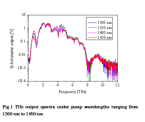
Figure 1 shows the collected THz output spectra under different pump wavelengths. THz radiation was generated at levels from less than 1 THz to more than 10 THz, with spectra that were almost independent of the pump wavelength proving Eq. 2 was right. When collinear phase matching is used to generate THz radiation, a deep dip in the spectra is observed at around 1.1 THz [1, 2]. This is suppressed here because the Cherenkov method results in surface emission, and we successfully obtained about 100 times higher signal compare to noise level of the detector. Additionally, radiation was generated below 1 THz, which cannot be generated using collinear phase matching with 1300-1450-nm pumping [3]. At frequencies above ~10 THz, the detection efficiency of the bolometer falls off, and this explains the low observed power at higher frequencies. However, the collected power extends to higher frequencies than were observed when using bulk lithium niobate in our previous works.
Although THz radiation generated far from the crystal-cladding interface interferes with that generated near the interface, resulting in destructive interference, the radiation generated deep within the crystal is attenuated due to the large absorption coefficient of the crystal. The absorption coefficient of DAST crystal at around 2-10 THz is 100-200 cm-1. The beam diameter was approximately 50 µm, and so the intensity of a THz-wave that propagates this distance will be attenuated by 30-60%. The output voltage of the Si bolometer can be converted to energy by considering that 1 V ≈ 20 pJ/pulse for low-repetition-rate detection and that we have a gain of 1000 at the bolometer. The highest-energy THz pulse obtained was about 50 pJ (3.3 mW at peak). The obtained output energy was higher than that of obtained by collinear phase matching condition using DAST crystal under almost same power density [1, 2].
3. Half cycle THz pulse generation using LiNbO3 crystal
As restricted by the temporal duration of the THz pulses used, the conventional axial resolution of THz tomography remains a few tens of microns. The common Å`10 µm thickness of coatings in various industrial products and the stratum corneum of human skin require higher depth resolution. The simple way to improve the axial resolution of tomographic imaging is by generating broadband and short THz pulses using shorter optical pulses. We have developed an all-fiber laser system that produces 17-fs optical pulses at a wavelength of 1.56 µm and have generated and detected broadband THz pulses ranging from 0.1 to 27 THz using DAST crystal. The temporal waveform of the generated THz pulses has several multiple peaks [4].
Here, we demonstrated spectral flat broadband THz pulse generation using thin LiNbO3 crystal under PCC-PM condition pumped by a fiber laser. The obtained temporal THz waveform was an ideal half cycle pulse which is suitable for reflection tomography. The experimental setup is shown in Fig. 2. The average power, pulse width, and repetition frequency of the pump fs fiber laser were 200 mW, 17 fs, and 48 MHz, respectively. The optical pulses were divided into two beams for THz wave generation and detection. The THz waves were radiated from a LiNbO3 plate (10Å~5Å~1 mm). The pump beam was tightly focused as close to the THz exit surface as possible using an asymmetrical lens with focal length of 11 mm.
The pump diameter before the asymmetrical lens was 1.2 mm (FWHM). A thin PET film was sandwiched between Si prism and LiNbO3 crystal to avoid pump leakage into Si. The THz pulses were detected by a 5-µm electrode gap LT-GaAs photoconductive antenna using parabolic mirrors. The temporal waveform of the THz waves was traced by scanning a delay stage whereby SHG pulses generated with a periodically- poled lithium niobate were used as probe pulses. The signal obtained was then fed into a preamplifier and detected with a lock-in amplifier. In this experiment, the THz wave path was not yet purged with dry nitrogen gas.
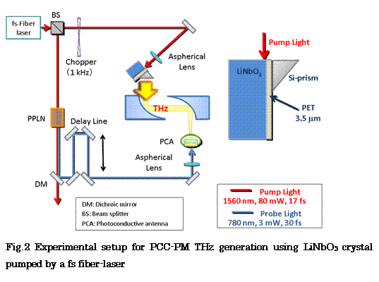
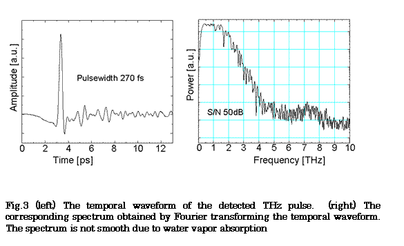
Figure 3 (left) shows the temporal waveform of the detected THz pulse. We successfully obtained half cycle THz pulse with pulsewidth of 270 fs. Fig. 3 (right) shows the corresponding spectrum obtained by Fourier transforming the temporal waveform. The spectrum extended up to 5 THz with almost Gaussian profile which leads to an ideal half cycle pulse.
[2]K. Suizu, K. Miyamoto, T. Yamashita, and H. Ito, ÅgHigh-power terahertz-wave generation using DAST crystal and detection using mid-infrared powermeter,Åh Opt. Lett. 32, 2885-2887 (2007).
[3]T. Taniuchi, S. Ikeda, S. Okada, and H. Nakanishi, ÅgTunable Sub-Terahertz Wave Generation from an Organic DAST Crystal,Åh Jpn. J. Appl. Phys. 44, L652-L654 (2005). J. Takayanagi, S. Kanamori, K. Suizu, M. Yamashita, T. Ouchi, S. Kasai, H. Ohtake, H. Uchida, N. Nishizawa, and K. Kawase, ÅgGeneration and detection of broadband coherent terahertz radiation using 17-fs ultrashort pulse fiber laser,Åh Opt. Express 16, 12859-12865 (2008).
D5. Photonic Millimeter-Wave Technology
H. Ito
Kitasato University
Photonic generation of millimeter (mm)/sub-millimeter (sub-mm) waves or terahertz (THz) waves is a promising technology since it offers an extremely wide bandwidth at very high frequencies, and is capable of low-loss transmission of these high-frequency signals through optical fibers. It is also advantageous for making the front-end component compact, light, and easy-to-handle for practical use. There are two major approaches in this technology, i.e., a pulsed operation of a device to simultaneously generate ultra-wideband frequency components, and a continuous-wave operation to generate a signal having extremely high spectral (or frequency) resolution with excellent stability. The former is often used for time-domain spectroscopy (TDS) employing low-temperature-grown GaAs photoconductors or nonlinear optical crystals. The latter is usually accomplished by photodiodes or nonlinear optical crystals, which offer relatively large average output power, less complex setup, and less sensitivity against environmental fluctuation.
Å@In reality, the use of long-wavelength (Å`1.55 µm) lights is important because we can use the abundant optical components developed for optical communications systems at a reasonable cost. To achieve such scheme, an efficient O/E conversion device (photomixer) with sufficiently high output power at very high frequencies is essential. The uni-traveling-carrier photodiode (UTC-PD) [1-3], developed in NTT laboratories, Japan, is one of the best solutions, because it provides a high 3-dB bandwidth and a high saturation output power simultaneously. To date, output powers of over 20 mW at 100 GHz, 0.5 mW at 350 GHz [4] and 10 µW at 1 THz have been achieved by the UTC-PD.
Å@In some applications, such as reflection-geometry spectroscopy, reflection-geometry imaging, and bi-directional wireless communications [5], it is important to use a compact transceiver head that has both transmitter and receiver functions. This makes the tight and therefore difficult optical alignment of the components much easier. For this purpose, a compact transceiver module that integrates a UTC-PD, a Schottky barrier diode [6], and a planar circulator circuit for operations at around 300 GHz [7] has been developed. All the components were assembled in a J-band (220-325 GHz) waveguide-output package.
Reflection-geometry THz imaging is suitable for security inspection and medical diagnosis since biological substances, such as human body, has large absorption coefficient due to containing water. Thus, the imaging was performed using the sub-THz transceiver module [7] mentioned above, and it was confirmed that a practical contrast could be obtained for a bandwidth of about 20 GHz. Based on these results, in-vivo imaging of a human finger was successfully demonstrated at 270 GHz.
Å@Another type of application is the TDS using pulsed mm-/sub-mm waves. For this purpose, a UTC-PD that is monolithically integrated with a coplanar waveguide (CPW) has been developed [8]. A sub-THz (pico-second) electrical pulse was generated by a UTC-PD and propagated through the CPW for the possible use in the proximity sensing of material properties including liquid samples. It was found that the higher-frequency Fourier components in the pulse remain considerably even after 2 mm propagation through the CPW fabricated on an InP substrate. These results demonstrated the possible use of the waveguide-integrated UTC-PD as a proximity THz-TDS device for, at least, up to 400 GHz.
Å@The photonic mm-wave ellipsometry system utilizing the UTC-PD has also been developed for revealing complex relative dielectric constant of the biological substances. This technique enables us to obtain more qualitative information of the material compared with the imaging, and the complex relative dielectric constant of human skin was successfully measured in-vivo in the F-band (90-140 GHz) [9]. Such information can only be obtained by the method other than the imaging, so that the complementary use of the imaging and the ellipsometry should be promising for analyzing the property of biological substances in the mm-/THz-wave range.
[2]T. Nagatsuma, H. Ito, and T. Ishibashi, ÅgHigh-Power RF Photodiodes and their Applications,Åh Laser and Photonics Reviews, vol. 3, No. 1-2, pp. 123-137, 2009.
[3]H. Ito, ÅgPhotonic Generation of Millimeter-/Terahertz-Waves using Uni-Traveling-Carrier Photodiodes,Åh Proc. Asia-Pacific Radio Science Conference (AP-RASC10), p. DC3-1, 2010.
[4]A. Wakatsuki, T. Furuta, Y. Muramoto, T. Yoshimatsu, and H. Ito, ÅgHigh-Power and Broadband Sub-Terahertz Wave Generation Using a J-Band Photomixer Module with Rectangular-Waveguide Output Port,Åh Proc. Int. Conf. on Infrared, Millimeter, and Terahertz Waves, pp. 1999-1-2, 2008.
[5]T. Nagatsuma, ÅgTowards 100-Gbit/s Wireless Using Terahertz Waves,Åh Extended Abst. Int. Workshop on Terahertz Technol., pp. 121-126, 2009.
[6]H. Ito, F. Nakajima, T. Ohno, T. Furuta, T. Nagatsuma, and T. Ishibashi, ÅgInP-Based Planar-Antenna-Integrated Schottky-Barrier Diode for Millimeter- and Sub-Millimeter-Wave Detection,Åh Jpn. J. Appl. Phys., vol. 47, No. 8, pp. 6256-6261, 2008.
[7]H. Ito, K. Yoshino, Y. Muramoto, H. Yamamoto, and T. Ishibashi, ÅgSub-Terahertz-Wave Transceiver Module Integrating Uni-Traveling-Carrier Photodiode, Schottky Barrier Diode, and Planar Circulator Circuit,Åh IEEE J. Lightwave Tech., vol. 28, No. 24, pp. 3599-3605, 2010.
[8]H. Ito, H. Yamamoto, T. Furuta, and T. Ishibashi, ÅgGeneration and Propagation of Sub-Terahertz Pulse Signal using Waveguide Integrated InP/InGaAs Uni-Traveling-Carrier Photodiode,Åh Jpn. J. Appl. Phys., vol. 49, No. 3, pp. 032402-1 - 032402-5, 2010.
[9]H. Yamamoto, H. Ito, and M. Noshiro, ÅgMillimeter-Wave Ellipsometry of Human Skin Based on Photonics Technology,Åh IEICE Electron. Express 7, No. 13, pp. 964-968, 2010.
D6. Plasmonic Device Technology for Emission and Detection of THz Radiation
T. Otsuji
Tohoku University
1. Introduction
ÅgTerahertzÅh is an unexplored electromagnetic frequency band staying in between microwaves and infrared lights in the sense that there is no commercially available microelectronic device that can generate and detect electromagnetic waves over the entire terahertz (THz) frequency band [1]. The terahertz frequencies fall in vibrations of most of molecules like water, protein, explosives, drugs, etc... Each substance has its own fingerprint in the terahertz frequency range. Therefore terahertz electromagnetic waves are capable of identifying the substance by using spectroscopic and/or imaging techniques; transmission/absorption spectra is identical to the substance so that terahertz radiation is powerful for those applications if a "compact," "room-temperature operating," "integrated solid-state" terahertz light source is developed. Presently, terahertz inspection instruments are being equipped at the security gates in several international airports. However their physical volume of the hardware is quite large due to the lack of "compact," "room-temperature operating," "integrated solid-state" terahertz light sources. The technology could be transferred to billions of consumer markets like portable/handy terahertz camera/scanner.
Å@The other aspect is the ultra-broadband/ultra-high-speed wireless communications [2]. Now mobile cellphones utilizes carrier frequencies around 3 GHz that can transfer data with 100-Mbit/s rate. It is insufficient to transfer HD-TV uncompressed video stream data. Soon or later Ultra-High Definition TV system will become in service which requires 3 orders higher data transmission rate. To accommodate such high capacity on the wireless comm. the carrier frequency should be increased in the terahertz (1000 GHz) range. Terahertz waves are severely absorbed by water vapors but short-distant transmission over 100 m is possible. If a compact, room-temperature operating solid-state terahertz light source is available, the terahertz wireless communication becomes in our hand indeed [2].
Å@In the last decade, development of compact, tunable and coherent sources operating at THz frequencies has been one of the hottest issues of the modern THz electronics. Conventional electron devices like field-effect transistors (FETs) increase their operating frequencies by scaling down the feature size, severely sacrificing the output power. Photonic devices like semiconductor lasers, on the other hand, decrease their operating frequencies by scaling down the transition energy from interband to inter-subband transition, severely suffering from the thermal noise. One can call such a difficult situation as ÅgTerahertz Gap.Åh[1]
Å@The channel of a FET can act as a resonator for plasma waves (collective electronic charge-density waves). When the plasma-wave frequencies are quantized into the resonances, we call such a quantum as Ågplasmon.Åh The plasmon frequency depends on its dimension and easily exceeds THz by setting the gate length in 100s nanometer scale. The study on applications of plasmon FETs for THz imaging/spectroscopy started at the early Åe90s with the pioneering theoretical work of Dyakonov and Shur [3, 4]. One of the severe issues to cope with, however, is the quantum efficiency: how to efficiently couple the non-radiative nature of plasmons to radiative electromagnetic waves.
2. Plasmon-Resonant Microchip Emitters
2.1. Device structure and operation
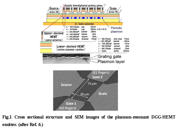
To circumvent such a problem, we have introduced an interdigitated dual grating gate (DGG) structure into a standard high-electron mobility transistor (HEMT) [5], shown in Fig. 1 [6]. The DGG can periodically localize the 2D plasmon in 100-nm regions with a micron interval. When the DC drain-to-source bias is applied, 2D electrons are accelerated to produce a constant drain-to-source current. Due to such a distributed plasmonic cavity systems in periodic 2D electron-density modulation, the DC current flow may excite the plasma waves in each plasmonic cavity, leading to self oscillation. The DGG acts also as a broadband THz antenna that converts non-radiative longitudinal plasmon modes to radiative transverse electromagnetic modes. Additionally, a vertical cavity structure is introduced in between the top DGG plane and a THz mirror at the backside, working as a plasmon-resonant enhancer [5, 6].
2.2. THz emission performance and applications
We have designed and fabricated our original plasmon-resonant emitters (PREs) using InGaP/InGaAs/GaAs material systems in a double-deck HEMT [6-8]. The intrinsic device area has a geometry of 30 É m x75 É m, where the DGG pattern is replicated on the upper-deck HEMT layer while the periodic plasmon cavities are configured on the lower-deck HEMT. The DGG consists of 150-nm and 1850-nm lines aligned alternately with a spacing of 100 nm. The number of DGG fingers is 37 (38) for the 1500-nm (1850-nm) grating. Experiments revealed the performances of the PREs exhibiting 1-É W broadband emission ranging from 0.5 to 6.5 THz at room temperature, shown in Fig. 2 [8].
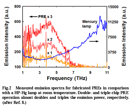
Compared with a commercially available high-pressure mercury (HP-Hg) lamp, the PRE exhibits a superior (two orders higher) energy conversion efficiency of 10-4 to 10-5 although the output power is by one order lower than the HP-Hg lamp5. We confirmed dual- and triple-chip operation of PREs successfully doubles and triples the emission intensity as shown in Fig. 2. The results encourage us to exceed the output power of the HP-Hg lamp by integrating the PREs in an array of 10 x 10 [8].
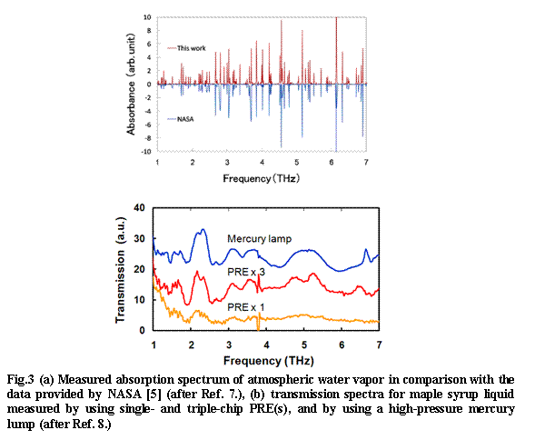
Å@The device is introduced as a light source into a Fourier-transform THz spectrometer. The water-vapor absorption lines are clearly observed with an excellent coincidence with the result provided by NASA5 as shown in Fig. 3(a) [7]. Fingerprints of several sugar-group materials in liquid are also successfully identified. As shown in Fig. 3(b), the poor S/N for a single-chip PRE operation is greatly improved by triple-chip operation, almost approaching the result using HP-Hg lamp [8].
3. Plasmon-Resonant THz Detectors
3.1. Device structure and operation
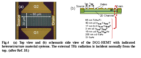
The plasmon resonant emitter device also works for a broadband high-sensitive THz detector [9]. Resent works done with collaboration with CNRS, Montpellier demonstrated excellent terahertz imaging hidden materials inside an envelope [9]. Our device structure is a InGaP/InGaAs/GaAs single-deck DGG-HEMT [5-8, 10] (see Fig. 4). The DGG is formed with 65-nm-thick Ti/Au/Ti by a standard lift-off process. Four different structures with a DGG were fabricated. The metal fingers of one grating gate G1 are of the same length LG1 = 100 nm in all structures, while grating gate G2 was designed to have fingers of different lengths LG2 = 300, 800, 1300, and 1800 nm for different structures. The spacing between the grating-gate fingers is 100 nm for all four structures. The whole length of the channel between the source and drain contacts covered by the DGG is about 80 µm with the channel width of 30 µm in each structure.
It is known that hydrodynamic nonlinearities in 2D electron channels can be used for detection of THz radiation [3]. Resonant THz detection is related to the excitation of high quality plasma waves (plasmons) in 2D electron channel, whereas a broadband non-resonant THz detection is related to overdamped plasmons in depleted regions of the channel. In the both resonant and non-resonant cases, THz photoresponse originates from the nonlinear dynamics of 2D electron fluid described by the hydrodynamic equations [3]


where E(x,t) is the in-plane electric field depending on the time t and coordinate x in 2D electron system, É— is the electron momentum relaxation time, j (x,t) = -e N(x,t)V(x,t) is the density of induced electric current, N(x,t) and V(x,t) are hydrodynamic electron density and velocity in 2D electron channel, and e and m* are the electron charge and effective mass, respectively. There are two different nonlinear terms in the system Eqs. (1) and (2): the second term in the Euler equation Eq. (1) describing the nonlinear electron convection in 2D electron fluid and the product N(x,t)V(x,t) defining the current density in the continuity equation Eq. (2). Time average of the nonlinear current yields the detection signal.
3.2. THz detection performance and applications
The transfer characteristics of the structure with LG2 = 300 nm are shown in the inset of Fig. 5 for drain-to-source voltage 0.5 V [10]. Each DGG structure was irradiated at normal incidence by THz beam at frequency 0.24 THz. We measured a photovoltaic DC response between the source and drain contacts (the source contact was grounded and no drain bias DC voltage was applied) at room temperature. Since the quality factor is estimated to be smaller than unity, É÷É— = 0.25, for the incident radiation frequency É÷/2ÉŒ = 0.24 THz, the non-resonant detection should be expected in our experiments at room temperature. Terahertz radiation was generated by a Backward Wave Oscillator (BWO) with maximum output power of 5 mW. The radiation was linearly polarized and chopped at 170 Hz. The radiation-induced photovoltage É¢U was measured as a function of the gate voltage UG1 or/and UG2 as 170 Hz ac voltage component of the source-to-drain voltage using the standard lock-in technique. Figure 5 demonstrates the photoresponse measured as a function of the gate voltage UG1 (for UG2 = 0) and that as a function of the gate voltage UG2 (for UG1 = 0) for the structure with LG2 = 300 nm when the THz electric field was directed across the grating-gate fingers (i.e., in the source-to-drain direction).
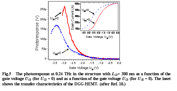
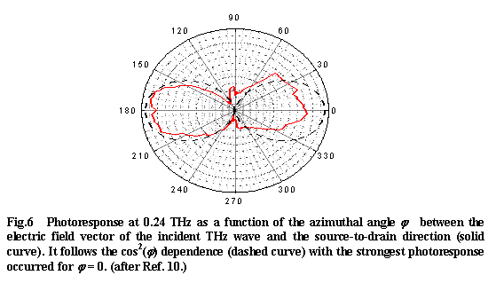
Figure 6 shows the dependence of the photoresponse on the azimuthal angle &fai; between the THz electric field and the source-to-drain direction for the structure with LG2 = 1300 nm [10]. The strongest photoresponse in all structures was observed when the electric-field vector of the incident THz wave was directed across the grating-gate fingers (i.e., in the source-to-drain direction). This demonstrates that the coupling between THz radiation and 2D electron channel is ensured by the DGG structure.
We performed raster-scan imaging in transmission mode with the measurement setup as shown in Fig. 7. The Gaussian-shaped focal spot has a radius of 710 É m. The power of the transmitted radiation is detected by our InP-HEMT with an active plasmonic gate length of 100 nm and a cutoff frequency of 268 GHz.
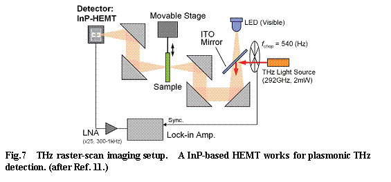
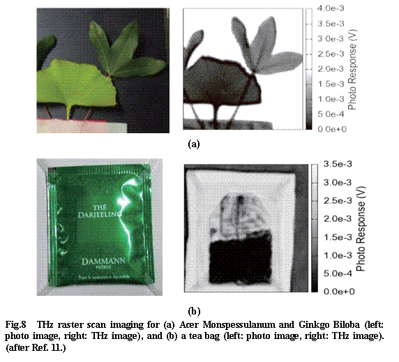
Figure 8 shows typical results for the samples (a) leaves which are called Acer Monspessulanum (Acer from Montpellier) and Ginkgo Biloba and (b) a tea bag with the package. The image of the leaves was successfully obtained with good contrast. From the image (b) and (c), the THz radiation transmitted through the package so that the tea leaves could be identified. The more water contains the more the THz radiation is absorbed, resulting in darker color. The amount of water contained in the tea bags appears in the images (b) and (c) as its darkness.
4. Conclusion
In conclusion the DGG-HEMT-based plasmon-resonant microchip emitters/detectors have been developed and revolutionized. Further improvements on its emission power and detection sensitivity by arrayed integration and/or novel breakthroughs like metamaterial antennae enable the device to be of a promising candidate of potential products of billions of consumer markets like portable/handy terahertz cameras/scanners as well as transmitters/receiver s for THz wireless communication systems.
[2] M. Dyakonov and M. Shur, Shallow water analogy for a ballistic field effect transistor: new mechanism of plasma wave generation by dc current, Phys. Rev. Lett. 71, 2465-2468 (1993). doi:10.1103/PhysRevLett.71.2465
[3] T. Nagatsuma, Challenges for ultrahigh-speed wireless communications using terahertz waves, International J. Terahertz Science and Technology, 3, 55-65 (2010).
[4] M. Dyakonov, and M. Shur, Detection, mixing, and frequency multiplication of terahertz radiation by two dimensional electronic fluid, IEEE Trans. Electron Devices 43, 380-387 (1996). doi:10.1109/16.485650
[5] T. Otsuji, M. Hanabe, T. Nishimura and E. Sano, A grating-bicoupled plasma-wave photomixer with resonant-cavity enhanced structure, Opt. Express 14, 4815-4825 (2006). doi:10.1364/OE.14.004815
[6] T. Otsuji, Y. M. Meziani, T. Nishimura, T. Suemitsu, W. Knap, E. Sano, T. Asano, V.V. Popov, Emission of terahertz radiation from dual-grating-gates plasmon-resonant emitters fabricated with InGaP/InGaAs/GaAs material systems, J. Phys.: Condens. Matter 20, 384206 (2008). doi:10.1088/0953-8984/20/38/384206
[7] Y. Tsuda, T. Komori, A. El Fatimy, T. Suemitsu, and T. Otsuji, Application of plasmonic microchip emitters to broadband terahertz spectroscopic measurement, J. Opt. Soc. Am. B 26, A52-A57 (2009). doi:10.1364/JOSAB.26.000A52
[8] T. Otsuji, "Plasmon-resonant microchip emitters and detectors for terahertz sensing and spectroscopic applications," Proc. SPIE. 7671, 767102 (2010).
[9] W. Knap, M. Dyakonov, D. Coquillat, F. Teppe, N. Dyakonova, J. Lusakowski, K. Karpierz, M. Sakowicz, G. Valusis, D. Seliuta, I. Kasalynas, A. El Fatimy, Y. M. Meziani, and T. Otsuji, Field effect transistors for terahertz detection: physics and first imaging applications, J. Infrared Milli. Terahz Waves 30, 1319-1337 (2009). doi:10.1007/s10762-009-9564-9
[10] D. Coquillat, S. Nadar, F. Teppe, N. Dyakonova, S. Boubanga-Tombet, W. Knap, T. Nishimura, T. Otsuji, Y. M. Meziani, G. M. Tsymbalov, and V. V. Popov, "Room temperature detection of sub-terahertz radiation in double-grating-gate transistors," Opt. Express 18, 6024-6032 (2010).
D7. Integrated Josephson Voltage Standard Technology
S. Kohjiro
National Institute of Advanced Industrial Science and Technology
Abstract
compact Programmable Josephson Voltage Standard (PJVS) system based on a cryocooler is under development at the National Institute of Advanced Industrial Science and Technology (AIST). Its key technology is a superconducting integrated circuit which generates the accurate voltage of 2 V based on the RF Josephson effect. The circuit chip consists of 65536 niobium-nitride-based Josephson junctions operating at 12 K, i.e., 3 times as large as the typical operating temperature of conventional niobium-based Josephson voltage standards. Since the PJVS chip requires cooling power of less than 100 mW, it is possible to use a compact-size cryocooler, which can be mounted inside a standard 19-inch rack-mount chassis. By combining the 2 V PJVS chip with a high-precision semiconductor voltage multiplier circuit, the accurate and arbitrary voltages up to 20 V are expected to be available not only to metrology institutes but also to manufacturing industries.
1. Introduction
Josephson junctions (JJs), junction sandwiches of superconductor/insulator (or normal conductor)/superconductor, exhibit equally spaced constant voltage steps on their voltage-current (V-I) curves under the irradiation of microwave of frequency f. Step voltages are given by

where m is the number of junctions in series, n the harmonics number, h PlanckÅfs constant, and e the unit charge. This means the voltage accuracy of JJs is in principle equal to the frequency accuracy of the microwave source and independent of temperature, humidity, materials of JJs, etc. From this reason, JJs are used for the primary DC voltage standard at national metrology institutes around the world. Because a JJ can produce only very small voltages of 10-200 µV, the array of 104-106 JJs should be developed to increase the output voltage up to ~10 V required as a calibration source for digital multimeters. Technologies of superconducting integrated circuits are necessary for JJ arrays with enough numbers of junctions and operating successfully.
Å@The Programmable Josephson Voltage Standard (PSVJ) systems [1-3] have the inherent advantages over the conventional Josephson voltage standard, i.e., shorter settling time (<1 É s) and larger voltage step width (>1 mA). Though the PJVS systems are now widely used as the primary voltage standards at national metrology institutes, semi-conductor (Zener) voltage standards are still the only choice for the secondary voltage standards. At the National Institute of Advanced Industrial Science and Technology (AIST), cryocooler-based PJVS systems have been under the development, utilizing the niobium-nitride-based (NbN/TiN/NbN) Josephson-junction arrays operating at 10 K [4,5]. This temperature is significantly higher than 4 K, at which conventional niobium (Nb)-based Josephson voltage standards operate.Å@Recently, the stable operation of the PJVS chip at 12 K has been demonstrated. The increase of 2 K in the operating temperature has enabled us the use of the smallest two-stage Gifford-McMahon (GM) cryocooler available on the market.
Å@This paper reports a low cost, compact PJVS system under development at the AIST, aiming to be a replacement for the conventional Zener secondary voltage standards.
2. System Description
The new PJVS system, designed as a secondary standard, requires periodical calibration by the primary standards, and need to be sufficiently compact for the transportation to the calibration institutes. To adopt a compact cryocooler which dominates both volume and power consumption of voltage standard system, two-stage voltage-output circuits are employed. The first-stage is a JJ array which produces accurate voltages of 0-2 V based on Eq. (1). The second-stage is a precision semiconductor voltage multiplier with a factor of 10. While the intrinsic accuracy of the PJVS will be degraded by the use of semiconductor circuits, it is still accurate enough for the secondary voltage standard.
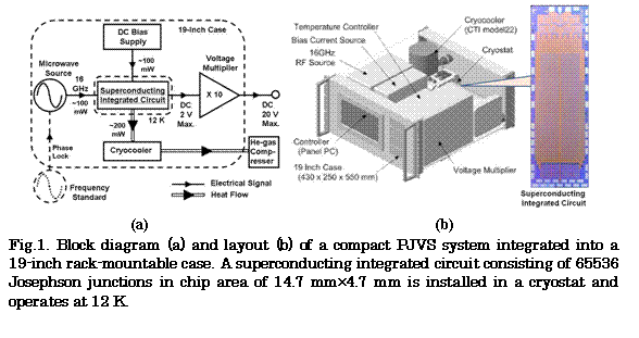
The dimensions of the smallest commercially available cryocooler (CTI model22) is 290 mmÅ~240 mmÅ~160 mm, which can be mounted into a 19-inch rack-mount chassis except for the helium(He)-gas compressor. Other system components to be assembled into the 19-inch rack-mount chassis are (1) a panel-mount PC as the system controller, (2) temperature controller to stabilize the operating temperature of the PJVS chip at 12K, (3) 24-channel bias current source, (4) 16GHz, 500mW microwave source, and (5) the Å~10 voltage multiplier circuit. The block diagram and layout of the compact PJVS system are shown in Fig. 1.
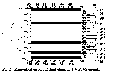
Fig. 2 shows an equivalent circuit of the dual-output 1-V PJVS circuit, where the total output voltage of the chip is 2 V. The microwave signal with f = 16 GHz is split into 16 arrays including 4096 NbN/TiN/NbN Josephson junctions each, and two of these have binary sub-arrays those work as digital-to-analog converters (DACs) with resolution of 10 bits. The polycrystalline NbN films for the electrode were prepared by an rf-magnetron sputter at ambient temperature on a 3-inch-diameter Si wafer, and the critical temperature of the 200-nm-thick NbN film was 15.9 K. The fabrication process was as same as that of a 10-V PJVS circuit except for the number of barriers per junction stack [6].
3. Experimental Results
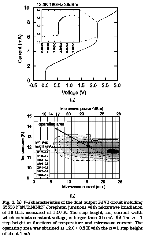
Fig. 3(a) shows a V-I characteristics of the dual-output PJVS circuit including 65536 NbN/TiN/NbN JJs with microwave irradiation of 16 GHz measured at 12.0 K. The constant voltage at 2.168 V is observed in the current width, i.e., step height, of 0.7 mA at 12.0 K, which is larger than the typical fluctuation of bias current due to external noise. Fig. 3(b) shows the operating area for the temperature and microwave current, where the current widths of both constant voltage steps of n=0 and n=1 are larger than 1 mA, i.e., the bias point is enough stable on the 1st step with typical external noise. The temperature range was about 1 K (12.0 Å} 0.5 K) and the microwave power range was about 3 dB (24.5 Å} 1.5 dBm).
4. Conclusion
A compact programmable Josephson voltage standard (PJVS) system using a 2 V PJVS chip is under development for the purpose of the new-generation secondary voltage standard with higher accuracy and less calibration frequency than present semiconductor (Zener) standards. It is demonstrated that the superconducting chip operates at 12 K with enough margins for the external noise. The chip requires moderate cooling power of ÅÉ100 mW, enabling the use of small-size cryocooler. All the main components of the PJVS systems, excluding the He-gas compressor, have been assembled inside a standard 19-inch rack-mountable case. By the use of a precision semiconductor voltage-multiplier circuit, the PJVS system can generate arbitrary voltages up to 20 V.
[2] S. P. Benz, C.A. Hamilton, C. J. Burroughs, T. E. Harvey, and L. A. Christian, Appl. Phys. Lett., vol. 71, p.1866 (1997).
[3] H. Schulze, R. Behr, J. Kohlmann, F. Mueller, and J. Niemeyer, Supercond. Sci. Technol., vol. 13, p. 1293 (2000).
[4] A. Shoji, H. Yamamori, M. Ishizaki, S. P. Benz, and P. D. Dresselhaus, IEEE Trans. Appl. Supercond. vol. 13, p. 919 (2003).
[5] H. Yamamori, T. Yamada, H. Sasaki, and A. Shoji, Supercond. Sci. Technol., vol.21, p. 105007 (2008).
[6] H. Yamamori, M. Ishizaki, A. Shoji, P. D. Dresselhaus, and S. P. Benz, Appl. Phys. Lett., vol. 88, p. 042503 (2006).
[7] H. Sasaki, H. Yamamori, T. Yamada, and A. Shoji, Ext. Abst. 12th International Superconductive Electronics Conference (ISECÅf09), HF-P10, June 16-19, Fukuoka, Japan (2009).
D8. High Capacity Optical Fiber Transmission Systems
H. Toda
Doshisha University
In this section, I summarize recent development of high capacity optical fiber transmission systems and related technologies.
Digital coherent technique is now indispensable for high capacity transmission systems. All of the experiments described here without notice are related to digital coherent. One of the recent trends is real-time coherent optical receiver and real-time digital signal processing [1, 2]. Compensation of impairments due to optical nonlinearity of transmission fiber is investigated [3, 4]. Error correction is important technique to greatly improve the performance of optical transmission systems [5]. Real-time FPGA prototype [6, 7] was demonstrated with soft decision LSI [8].
Å@For ultra-high capacity systems, 69.1 Tbit/s (432 WDM x 171-Gbit/s) transmission over 240 km was demonstrated using PDM-16-QAM modulation [9]. High optical spectral efficiency can be achieved with multi-level modulation format. 6.4 bit/s/Hz with PDM 16-QAM [10], 9.0 bit/s/Hz with PDM 64-QAM [11], 11.9 bit/s/Hz with PDM 256-QAM [12], and 13.2 bit/s/Hz with PDM 512-QAM [13] were obtained. On the contrary, a review of direct-detection (incoherent) multi-level modulation scheme as a simple alternative to the coherent schemes was made in [14]. Optical QAM signal can be obtained with an optical IQ modulator, which is used for optical QPSK modulation, driven by multi-level electrical signals. Efforts have been made to generate optical QAM signal with a single dual-drive Mach Zehnder modulator [15]. Other efforts are being made to realize optical QAM modulator for high baud-rate QAM modulation. A hybrid configuration of silica planar lightwave circuit and LiNbO3 phase modulators for 64 QAM modulation [16], and monolithically integrated quad Mach-Zehnder IQ modulator for 16 QAM modulation [17] are demonstrated.
Å@Multi-core fiber [18, 19] is also one of the key trends for increasing transmission capacity. Efforts are being made for reducing propagation loss and inter-core crosstalk. Very recently, record transmission capacity of 109 Tbit/s was achieved by using multi-core fiber. Modulation format used in that experiment was QPSK. Therefore, increase of the transmission capacity can be easily expected if more advanced modulation format is used.
Å@CO (coherent optical) -OFDM has been studied for optical fiber transmission systems because of its high dispersion tolerance and high spectrum efficiency [20, 21]. 10 WDM x 121.9-Gbit/s transmission is demonstrated over 1,000-km standard single mode fiber without any inline dispersion compensation [22]. 7.0-bit/s/Hz spectral efficiency was obtained with 32-QAM subcarrier modulation [23]. No guard-interval CO-OFDM scheme was demonstrated for ultimate spectral efficiency [24, 25]. 13.5 Tbit/s (135 WDM x 111-Gbit/s) transmission over 6,248 km was demonstrated by the use of distributed Raman amplification [26]. Bit-rate-flexible all-optical OFDM transceiver [27] and integrated-optic OFDM demultiplexer [28] were demonstrated.
Å@For ultra-high speed transmission, OTDM can be used in conjunction with the digital coherent technique [29]. 640 Gbit/s dual-polarization QPSK transmission [30, 31] was demonstrated. For incoherent system, 640 Gbit/s single-polarization DPSK transmission with time-domain optical Fourier transformation was demonstrated [32].
Å@New wavelength of 1É m region for optical fiber communication is exploited with photonic crystal fiber [33, 34], while applicability to conventional telecommunication band is investigated [35, 36]. Efforts are continuously being made to obtain low propagation loss and enlarged effective area [37].
List of Abbreviations
DPSKÅ@Å@Å@Differential Phase-Shift Keying
FPGAÅ@Å@Å@Field-Programmable Gate Array
OFDMÅ@Å@Å@Orthogonal Frequency Division Multiplexing
OTDMÅ@Å@Å@Optical Time Division Multiplexing
PDMÅ@Å@Å@Polarization Division Multiplexing
QAMÅ@Å@Å@Quadrature Amplitude Modulation
QPSKÅ@Å@Å@Quadrature Phase-Shift Keying
WDMÅ@Å@Å@Wavelength Division Multiplexing
References
[2] T. Tanimura, Y. Aoki, H. Nakashima, T. Hoshida, J. Li, Z. Tao, and J. C. Rasmussen," FPGA-based 112Gb/s coherent DP-QPSK receiver and multi-stage PMD-PDL emulator for fast evaluation of digital signal processing algorithms," Tech. Digest of ECOC 2010, Tu.5.A.3, Torino, Sept. 19-23, 2010.
[3] S. Oda, T. Tanimura, T. Hoshida, C. Ohshima, H. Nakashima, Z. Tao, and J. C. Rasmussen, "112 Gb/s DP-QPSK transmission using a novel nonlinear compensator in digital coherent receiver," Tech. Digest of OFC/NFOEC 2009, OThR6, San Diego, Mar. 22-26, 2009.
[4] T. Hoshida, T. Tanimura, S. Oda, T. Tanaka, H. Nakashima, Z. Tao, L. Li, L. Liu, W. Yan, and J. C. Rasmussen, "Recent progress on nonlinear compensation technique in digital coherent receiver," Tech. Digest of OFC/NFOEC 2010, OTuE5, San Diego, Mar. 21-25, 2010.
[5] F. Chang, K. Onohara, and T. Mizuochi, "Forward error correction for 100 G transport networks," IEEE Commun. Mag., vol. 48, no. 3, pp. S48-S55 , 2010.
[6] T. Mizuochi, Y. Konishi, Y. Miyata, T. Inoue, K. Onohara, S. Kametani, T. Sugihara, K. Kubo, T. Kobayashi, H. Yoshida, and T. Ichikawa, "FPGA based prototyping of next generation forward error correction," Tech. Digest of ECOC 2009, 5.4.1, Vienna, Sept. 20-24, 2009.
[7] T. Mizuochi, Y. Konishi, Y. Miyata, T. Inoue, K. Onohara, S. Kametani, T. Sugihara, K. Kubo, H. Yoshida, T. Kobayashi, and T. Ichikawa, "Experimental demonstration of concatenated LDPC and RS codes by FPGAs emulation," IEEE Photon. Tech. Lett., vol. 21, no. 18, pp. 1302-1304 (2009).
[8] T. Kobayashi, S. Kametani, K. Shimizu, K. Onohara, H. Tagami and T. Mizuochi, "Soft decision LSI Operating at 32 Gsample/s for LDPC FEC-based optical transmission systems," Tech. Digest of OFC/NFOEC 2009, OWE2, San Diego, Mar. 22-26, 2009.
[9] A. Sano, H. Masuda, T. Kobayashi, M Fujiwara, K. Horikoshi, E. Yoshida, Y. Miyamoto, M. Matsui, M. Mizoguchi, H. Yamazaki, Y. Sakamaki, and H. Ishii, "69.1-Tb/s (432 x 171-Gb/s) C- and extended L-band transmission over 240 km using PDM-16-QAM modulation and digital coherent detection,Åh Tech. Digest of OFC/NFOEC 2010, PDPB7, San Diego, Mar. 21-25, 2010.
[10] S. Yamanaka, T. Kobayashi, A. Sano, H. Masuda, E. Yoshida, Y. Miyamoto, T. Nakagawa, M. Nagatani, and H. Nosaka, "11 x 171 Gb/s PDM 16-QAM transmission over 1440 km with a spectral efficiency of 6.4 b/s/Hz using high-speed DAC," Tech. Digest of ECOC 2010, We.8.C.1, Torino, Sept. 19-23, 2010.
[11] A. Sano, T. Kobayashi, A. Matsuura, S. Yamamoto, S. Yamanaka, E. Yoshida, Y. Miyamoto, M. Matsui, M. Mizoguchi, and T. Mizuno, "100 x 120-Gb/s PDM 64-QAM transmission over 160 km using linewidth-tolerant pilotless digital coherent detection," Tech. Digest of ECOC 2010, PD2.4, Torino, Sept. 19-23, 2010.
[12] M. Nakazawa, S. Okamoto, T. Omiya, K. Kasai, and M. Yoshida, "256-QAM (64 Gb/s) coherent optical transmission over 160 km with an optical bandwidth of 5.4 GHz," IEEE Photon. Tech. Lett., vol. 22, no. 3, pp. 185-187, 2010.
[13] S. Okamoto, K. Toyoda, T. Omiya, K. Kasai, M. Yoshida and M. Nakazawa, "512 QAM (54 Gbit/s) coherent optical transmission over 150 km with an optical bandwidth of 4.1 GHz," Tech. Digest of ECOC 2010, PD2.3, Torino, Sept. 19-23, 2010.
[14] N. Kikuchi, "Direct-detection high-speed multilevel signalling with digital signal processing," Tech. Digest of ECOC 2010, We.6.A.3, Torino, Sept. 19-23, 2010.
[15] S. Kametani, T. Sugihara, and T. Mizuochi, "16-QAM modulation by polar coordinate transformation with a single dual drive Mach-Zehnder modulator," Tech. Digest of OFC/NFOEC 2009, OWG6, San Diego, Mar. 22-26, 2009.
[16] H. Yamazaki, T. Yamada, T. Goh, Y. Sakamaki, and A. Kaneko, "64QAM modulator with a hybrid configuration of silica PLCs and LiNbO3 phase modulators for 100-Gb/s applications," Tech. Digest of ECOC 2009, 2.2.1, Vienna, Sept. 20-24, 2009.
[17] G. -W. Lu, T. Sakamoto, A. Chiba, T. Kawanishi, T. Miyazaki, K. Higuma, M. Sudo, and J. Ichikawa, "16-QAM transmitter using monolithically integrated quad Mach-Zehnder IQ modulator," Tech. Digest of ECOC2010, Mo.1.F.3, Torino, Sept. 19-23, 2010.
[18] K. Imamura, K. Mukasa, and T. Yagi, "Investigation on multi-core fibers with large Aeff and low micro bending loss," Tech. Digest of OFC/NFOEC 2010, OWK6, San Diego, Mar. 21-25, 2010.
[19] T. Hayashi, T. Nagashima, O. Shimakawa, T. Sasaki, And E. Sasaoka, "Crosstalk variation of multi-core fibre due to fibre bend," Tech. Digest of ECOC 2010, We.8.F.6, Torino, Sept. 19-23, 2010.
[20] S. L. Jansen, I. Morita, T. C. W. Schenk, and H. Tanaka, "121.9-Gb/s PDM-OFDM transmission with 2-b/s/Hz spectral efficiency over 1000 km of SSMF," IEEE/OSA J. Lightwave Technol., vol. 27, no. 3, pp. 177-188 (2009).
[21] T. Kobayashi, A. Sano, E. Yamada, E. Yoshida, and Y. Miyamoto, "Over 100 Gb/s electro-optically multiplexed OFDM for high-capacity optical transport network,Åh IEEE/OSA J. Lightwave Technol., vol. 27, no. 16, pp. 3714-3720 (2009).
[22] S. L. Jansen, I. Morita, and H. Tanaka, "10x121.9-Gb/s PDM-OFDM transmission with 2-b/s/Hz spectral efficiency over 1,000 km of SSMF, Tech. Digest of OFC/NFOEC 2008, PDP2, San Diego, Feb. 24-28, 2008.
[23] H. Takahashi, A. A. Amin, S. L. Jansen, I. Morita, and H. Tanaka, "Highly spectrally efficient DWDM transmission at 7.0 b/s/Hz using 8 x 65.1-Gb/s coherent PDM-OFDM, IEEE/OSA J. Lightwave Technol., vol. 28, no. 4, pp. 406-414 (2010).
[24] E. Yamada, A. Sano, H. Masuda, T. Kobayashi, E. Yoshida, Y. Miyamoto, Y. Hibino, K. Ishihara, Y. Takatori, K. Okada, K. Hagimoto, T. Yamada, and H. Yamazaki, "Novel no-guard-interval PDM CO-OFDM transmission in 4.1 Tb/s (50 x 88.8-Gb/s) DWDM link over 800 km SMF including 50-GHz spaced ROADM nodes," Tech. Digest of OFC/NFOEC 2008, PDP8, San Diego, Feb. 24-28, 2008.
[25] A. Sano, E. Yamada, H. Masuda, E. Yamazaki, T. Kobayashi, E. Yoshida, Y. Miyamoto, R. Kudo, K. Ishihara, and Y. Takatori, "No-guard-interval coherent optical OFDM for 100-Gb/s long-haul WDM transmission," IEEE/OSA J. Lightwave Technol., vol. 27, no. 16, pp. 3705-3713 (2009).
[26] H. Masuda, E. Yamazaki, A. Sano, T. Yoshimatsu, T. Kobayashi, E. Yoshida, Y. Miyamoto, S. Matsuoka, Y. Takatori, M. Mizoguchi, K. Okada, K. Hagimoto, T. Yamada, and S. Kamei, "13.5-Tb/s (135 x 111-Gb/s/ch) no-guard-interval coherent OFDM transmission over 6,248 km using SNR maximized second-order DRA in the extended L-band," Tech. Digest of OFC/NFOEC 2009, PDPB5, San Diego, Mar. 22-26, 2009.
[27] K. Yonenaga, F. Inuzuka, S. Yamamoto, H. Takara, B. Kozicki, T. Yoshimatsu, A. Takada, and M. Jinno, "Bit-rate-flexible all-optical OFDM transceiver using variable multi-carrier source and DQPSK/DPSK mixed multiplexing," Tech. Digest of OFC/NFOEC 2009, OWM1, San Diego, Mar. 22-26, 2009.
[28] K. Takiguchi, T. Kitoh, A. Mori, M. Oguma, and H. Takahashi, "Integrated-optic OFDM demultiplexer using slab star coupler-based optical DFT circuit, Tech. Digest of ECOC 2010, PD1.6, Torino, Sept. 19-23, 2010.
[29] C. Zhang, Y. Mori, K. Igarashi, K. Katoh, and K. Kikuchi, "Ultrafast operation of digital coherent receivers using their time-division demultiplexing function," IEEE/OSA J. Lightwave Technol., vol. 27, no. 3, pp.224-232 (2009).
[30] C. Zhang, Y. Mori, K. Igarashi, and K. Kikuchi, Demodulation of 640-Gbit/s polarization-multiplexed OTDM QPSK signals using a digital coherent receiver," Tech. Digest of OFC/NFOEC 2008, PDP6, San Diego, Feb. 24-28, 2008.
[31] C. Zhang, Y. Mori, M. Usui, K. Igarashi, K. Katoh, and K. Kikuchi, "Straight-line 1,073-km transmission of 640-Gbit/s dual-polarization QPSK signals on a single carrier," Tech. Digest of ECOC 2009, PD2.8, Vienna, Sept. 20-24, 2009.
[32] T. Hirano, P. Guan, T. Hirooka, and M. Nakazawa, "640 Gbit/s single-polarization DPSK transmission over 525 km with time-domain optical Fourier transformation in a round-trip configuration," Tech. Digest of OFC/NFOEC 2010, OThD7, San Diego, Mar. 21-25, 2010.
[33] R. Katouf, N. Yamamoto, K. Akahane, T. Kawanishi and H. Sotobayashi, "1-É m band transmission by use of a wavelength tunable quantum-dot laser over a hole-assisted fiber, SPIE Photonics West, 7234-14, San Jose, Jan. 24-29, 2009.
[34] K. Koizumi, M. Yoshida, T. Hirooka, and M. Nakazawa, "10 Gbit/s photonic crystal fiber transmissions with 1.1 É m directly-modulated single-mode VCSEL, Tech. Digest of OFC/NFOEC 2010, OWK3, San Diego, Mar. 21-25, 2010.
[35] T. Matsui, K. Nakajima, and C. Fukai, "Applicability of photonic crystal fiber with uniform air-hole structure to high-speed and wide-band transmission over conventional telecommunication bands," IEEE/OSA J. Lightwave Technol., vol. 27, no. 23, pp. 5410-5416 (2009).
[36] K. Mukasa, K. Imamura, R. Sugizaki and T. Yagi, "Comparisons of merits on wide-band transmission systems between using extremely improved solid SMFs with Aeff of 160É m2 and loss of 0.175dB/km and using large-Aeff holey fibers enabling transmission over 600nm bandwidth," Tech. Digest of OFC/NFOEC 2008, OThR1, San Diego, Feb. 24-28, 2008.
[37] T. Matsui, T. Sakamoto, K. Tsujikawa, and S. Tomita, "Single-mode photonic crystal fiber with low bending loss and Aeff of > 200 É m2 for ultra high-speed WDM transmission,Åh Tech. Digest of OFC/NFOEC 2010, PDPA2, San Diego, Mar. 21-25, 2010.
D9. Radio-on-Fiber Technologies for Heterogeneous Wireless Services
K. Tsukamoto
Osaka University
1. Introduction
Ubiquitous network should offer users the environment to access any communication service at any time, any place, and any situations. The demand of users for various multimedia services will be increasing more and more; therefore full IP connectivity will be required to accommodate the variety of contents. However, such diversification appears not only in application services but also in air interfaces of wireless access methods. The heterogeneous wireless networks also strongly depend on usersÅf different demands for applications, quality, latency, and moreover usersÅf situations such as indoor, outdoor, and fast/slow mobility. Therefore, the platform for heterogeneous wireless network will become a key issue to realize ubiquitous networks.
Å@In current wireless networks, various operators independently overlaid their own radio base stations and networks. This leads redundant equipments and investments on infrastructures, and prevents the quick start of a new wireless service. From the viewpoint of the improvement in the radio frequency utilization, microcellular or picocellular architecture is much effective, however, the implementation of different types of base stations and networks provided by different operators prevent them from adopting microcellular due to its large investment. Therefore, the future ubiquitous wireless networks will need a cross frequency platform, which can be commonly used by various types of wireless services under the multi-air interferences coexistence. In addition, various kinds of high-throughput mobile internet services should be provided at any time and any place. It will be requested that mobile throughput should be equivalent to the optical fiber internet access service up to Gigabit per second [1-4]. The radio regulation (RR) strictly also limits the transmitting power and bandwidth of RF signal. The higher radio frequencies will be assigned to new wireless services because of the lack of bandwidth at present. The new higher radio frequency bands such as microwave, millimeter wave, and terahertz-wave are promising as resources for higher-throughput wireless local/personal area networks. To accommodate a large number of access points, and also increasing mobile traffic as increased opportunities accessing to mobile video streaming, HDV download, wireless cloud services, or so on, advanced FMC (fixed and mobile convergence) between broadband optical access and mobile access, will become more and more important [5].
RoF (Radio on Fiber) technologies are available to realize a universal platform for transparent forwarding various types of wireless services under the multi-air-interferences coexistence in wireless cloud service environments. To realize future user centric wireless cloud service networks, software definable radio network (SDRN) has been proposed [6], that can be configured with the combination of RoF entrance networks, software definable radio gateway, wireless service over IP, and radio agents.
2. Radio on Fiber Technologies
Radio on Fiber (RoF) link shown in Fig. 1 has a function of transferring radio signals into remote stations with keeping their radio formats. Consequently, RoF link becomes a hopeful candidate of a common platform for various wireless access networks. For example, mobile carriers have widely installed RoF feeder systems in underground, in-building, and tunnels to solve the dead zone problems in these areas [7-8] as shown in Fig. 2. Especially, in public spaces such as underground stations and shopping center, three carriers commonly use a RoF feeder to provide 2G (800MHz, 1.5GHz) and 3G (2GHz) services together in Japan. For broadcasting applications, some feasibility experiments have been executed for TTL SFN relay link [9], power-supply less RoF repeater for terrestrial SFN [10] and gap filler systems in rural areas for terrestrial digital broadcasting. Recently, gap filler systems for mobile reception of one-segment digital TV have been applied in underground [11]. Reference [12] summarizes various applications of RoF technologies in mobile communications and broadcasting systems.
Recently, RoF applications has been developed to solve digital divide problem. Reference [13] reported the convergence project of RoF and CATV which was experimentally demonstrated the simultaneous transmission of ISDB-T, WiMAX, and WiFi signals into rural areas where broadband fiber-infrastructures have not yet been constructed due to their high cost and a low population. A similar convergence of RoF and CATV, which is called as RFoG (Radio Frequency over Glass) has been approved as a standard of the Society of Cable and Telecommunications Engineers (SCTE), SCTE 174 2010. RFoG has started to be demonstrated in urban optical CATV systems. In order to improve the transmission quality of RF signals against nonlinearities or reflection noises in RoF link, recently, digital RoF systems have been developed [14].
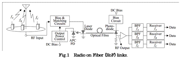
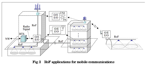
When RoF equips photonic routing functions, any radio signal can be forwarded to its destination control station [6]. Such RoF networks have been called as ÅgVirtual Radio Free Space Network (VRFSN)Åh. By the use of RoF, the radio access architecture can easily employ microcell, picocell or femtocell systems. Then, the RBS in each radio zone equips only the converter between radio and optical signals. The RBS requires neither the modulation functions nor demodulation functions of radio signals. The radio signals converted into optical signals are transmitted via a RoF link with the benefit of its low transmission loss and broadband. Therefore, RoF links can be independent of the radio signals format and can provide many universal radio access methods. This means that VRFSNs are very flexible to the modification of radio signal formats, the opening of new radio services, or the accommodation of some different types of radio signal formats. A remote radio control station (RCS) executes functions of modulation and demodulation of radio and other controls such as channel allocations, hand over processing and so on. Such concentrated execution of their complicated function makes radio access networks more simplified and cost effective, and promises easy realization of recent advanced radio techniques, such as hand over control, or interference cancellations.
Å@Universal RBSs and entrance links mean a realization of layer 1 routing shown in Fig. 3, that is especially effective in private areas at in-house, in-building, and underground at urban areas, and rural areas with no broadband fiber-infrastructures and a low population. The layer 1 routing can be also realized RoFSO (Radio on Free Space Optics) [15, 16] or RoR (Radio on Radio)[6] networks, which can provide a free space for heterogeneous wireless services in Free Space Optics or millimeter wave radio. In each network, radio signals are converted into optical free-space optic signals or MMW signals with wideband frequency conversion.
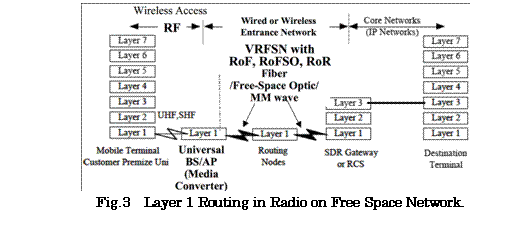
3. Software Definable Radio Networks
Figure 4 illustrates the concept of extended VRFSN, called Software Definable Radio Network (SDRN) and its configuration [6]. The SDRN is composed with Radio on Free Space (RoFSx) networks, universal RBS and software definable control server (SDRCS) in IP network for various types of wireless services, and SDRGW (Software Definable Radio Gateway), which provides a seamless connectivity between local RoF networks and IP network. Followings are features:
1)Virtual Radio Free Space Transporting Networking: RoFSx (Fiber, Optics, Radio, and LCX etc) networks can transparently connect multi-dimensional radio spaces with photonic intensity (1 dimension).
ÅE Universality for multi carrier operation: Various types of radio terminals can access a RBS, and their RF signals are transparently transported in a RoFSx network, which provides a transparent entrance network between RBS and IP network, implements virtual free spaces for any radio signals in fiber, FSO, and MMW by equipping routing function to transfer the radio signal to its desirable SDRGW.
ÅE SDRGW and WoIP: SDRGW has functions of air-interface conversion and IP packeterization of wireless data and control signals. The later function is that the datagram in any radio signal are converted to IP packet, which are transported to its center station altogether with the control channel signal. This can realize a global cross layer platform on the IP network for heterogeneous wireless services networks, called ÅgWireless Service over IP (WoIP)Åh [6]. DRoF techniques is effective to realize RF signals over IP networks, where various types of wireless services can be transparently supported by using IP routing abilities[17]
2) Heterogeneous Radio Smart Space Construction: RoFSx networks can easily provide microcellular architecture, and have an ability of delivering appropriate radio frequency resources to users with the minimum power at any place and any time. With several distributed universal BS, macro diversity reception, interference canceling, or SDMA can be easily realized. Therefore, more improvement in the frequency efficiency can be expected.
3) User Centric Radio Space Control Agent: The SDRN can realize an easy spectrum delivery to users, but its operation should be performed not only to enhance frequency efficiency but also to satisfy usersÅf and operatorsÅf demands. Even if accessing the same wireless services, user utilities depend on their mobility and situations. In order to realize such seamless session handover or service handover in heterogeneous wireless, we need the Radio Agent on Layer 7, which controls layer 1-3 according to usersÅf and operatorsÅf demands, and radio regulations.
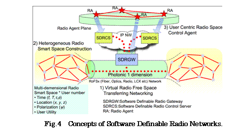
4. Ubiquitous antenna architecture distributed by RoF
As for the recent wireless radio technology, multi-antenna technologies are used in almost all new wireless radio access such as MIMO (multiple-input multiple-output) towards high throughput and high reliable communication [18-20]. The heterogeneous wireless access is effective to achieve higher data rate and wider area coverage. RoF is effective to construct heterogeneous networks to provide wireless cloud services with low cost. Figure 5 illustrates MIMO system with ubiquitous antenna distributed by RoF. The ubiquitous antenna system is a kind of distributed antenna system (DAS) using RoF network [21-28]. This network is constructed with a centralized control station (CCS) and plural remote antenna elements connected with CCS via RoF link. A remote antenna element haa only a function as a media converter that provides radio-to-optical (R/O) and optical-to-radio (O/R) conversion. The other functions of radio modulation, demodulation, diversity, and handover are processed in the CCS. Especially in MIMO, multiplexing and decomposition process of plural spatial streams is processed at the CCS. At the remote antenna, heterogeneous RF services are transmitted for heterogeneous wireless services. In this configuration, the separation among multiple antenna elements can be easily expanded so that MIMO spatial filtering process overcome correlated fading channel [18, 26].
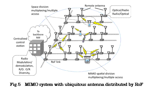
Therefore, the distributed MIMO antenna can increase the throughput in cell because it emphasize rich scattering environment and reduce the correlation among four signals over wireless multipath channels [18, 26].
Å@Recently, reference proposed a new configuration for RoF-MIMO DAS over WDM-PON, and reported some results of basic experimental examination. Fully utilization of optical wavelength resources is effective to accommodate a lot of remote station that are required for RoF-MIMO DAS with higher wireless capacity. Since the capacity of a wavelength channel is large enough for heterogeneous wireless signals, such as various types of wireless services, different radio frequency, some RF signals with different destinations. Then, multiplexing method is required for not only remote antennas, but also RF services. References proposes a new architecture to multiplexing method on RoF link based on the combination of optical time division multiplexing (OTDM) and wavelength division multiplexing (WDM).
[2] W-T. Shaw, et al., ÅgAn Ultra-Scalable Broadband Architecture for Municipal Hybrid Wireless Access Using Optical Grid NetworkÅh, OFC/NFOEC 2009, OThP2 (March, 2009).
[3] K. Iwatsuki, et al., ÅgAccess and Metro Networks based on WDM Technologies,Åh IEEE JLT, 22, no.11, pp.2623-2630 (2004).
[4] K. Iwatsuki, ÅgApplication and Technical Issues of WDM-PON,Åh SPIE, OptEast, 7620-11, (2010).
[5] Junichi Kani, ÅgTrends in Next Generation Optical Access Networks and a Proposed Hybrid Optical/wireless Wide-area Access Network,Åh PIERS Online, Vol. 4, No. 1, 101-105, (2008).
[6] S. Komaki, ''Microwave Technologies for Software Radio Networks'', Proceedings of APMC2003, Vol.3, No.FC7-1, pp.1780-1785 (November 2003).
[7] Y. Ito and Y. Ebine: ÅgRadio on Fiber System for Triple Band Transmission in Cellular Mobile CommunicationÅh, Tech. Digest of Int. Topical Meeting on Microwave Photonics, MWP 2000, TU1.2 Oxford, pp.35-38 (2000).
[8] Y. Horiuchi, ÅgROF Application to 3G Mobile Systems in Offices and Outdoors,Åh MWP 2005, p.3, Oct. 2005.
[9] M. Maeda, NHK STRL R&D No.90, pp.28-39 (March 2005).
[10] Y. Toba, et. al., "Development of a wide dynamic ranged radio wave receiving systems with an optical modulators and DFB laser", IEICE Trans. on Elec., Vol.J88-C, No.2, pp.99-106 (2005).
[11] http://www.nhkitec.co.jp/001topics/2005/002/index
[12] T. Kuri , Y. Horiuchi , T. Nakatogawa , and K. Tsukamoto: ''Communication and Broadcasting Systems with Microwave and Millimeter-Wave Photonics Technologies'', IEICE Transactions on Electronics, Vol.J91-C, No.1, pp.11-27, (January 2008) in Japanese.
[13] K. Kumamoto, K. Yasukawa1, K. Inagaki, T. Higashino, K. Tsukamoto, and S. Komaki :''CONVERGECE OF BROADCASTING AND COMMUNICATION UTLIZING CATV NETWORK'', Proc. of URSI AP-RASC2010, Toyama, Vol.1, No.DC2-3, p.1 (September 2010).
[14]A. Nirmalathas, P. A. Gamage, C. Lim, D. Novak, R. Waterhouse, and Y. Yang,ÅgDigitized RF transmission over FibersÅh, IEEE Microwave Magazine, June, pp.75-81 (2009)
[15] Kamugisha Kazaura, Kazuhiko Wakamori, Mitsuji Matsumoto, Takeshi Higashino, Katsutoshi Tsukamoto, and Shozo Komaki :''RoFSO : A Universal Platform for Convergence of Fiber and Free-Space Optical Communication Networks'', IEEE Communications Magazine, Vol.48, No.2, pp.130-137 (February 2010).
[16] Katsutoshi Tsukamoto, Akira Hashimoto, Yuji Aburakawa, and Mitsuji Matsumoto :''The case for free space - Exploring the prospect of free-space optical links for backhaul applications-'', IEEE Microwave Magazine, Vol.10, No.5, pp. 84-92 (August 2009).
[17] Bo Hu, Takeshi Higashino, Katsutoshi Tsukamoto, and Shozo Komaki :''Proposal of an RF Transmission over the IP Based Network and its SNR Performance Evaluation'', Proc. of Asia-Pacific Microwave Photonic Conference (APMP)2009, Vol.1, No.63, pp.1-4, (April 2009).
[18] A. Van Zelst and J. Hammerschmidt, ÅgA Single Coefficient Spatial Correlation Model for Multiple-input Multiple-output MIMO Radio Channel,Åh Proc. of URSI-GA, vol.1 (August, 2002).
[19] E. Biglieri, R. Calderbank, A. Constantinides, A. Goldsmith, A. Paulraj, H.V. Poor, MIMO Wireless Communications, Cambridge University Press, New York (2007).
[20] S. Karachontzitis, and D. Toumpakaris, ÅgEfficient and Low-cost Complexity User Selection for the Multiuser MISO Downlink, Åh Proc. of PIMRC2009, vol.1, no.1, pp.1-5 (Sep. 2009).
[21] A. Kobyakov, D. Thelen, A. Chamarti, M. Sauer, and J. Winters, ÅgMIMO Radio Signals over Fiber in Picocells for Increased WLAN Coverage,Åh Proc. of OFC/NFOEC 2008.
[22] S.P. Monteiro, N.J. Gomes, A. Gameiro, and T. Kawanishi, ÅgNext-generation Distributed and Heterogeneous Architectures: The FUTON Project,Åh Proc. of APMP2009, vol.1, no.1, pp.1-4 (April 2009).
[23] C. Liu, and A. Seeds, ÅgTransmission of MIMO Radio Signals over Fibre Using a Novel Phase Quadrature Double Sideband Frequency Translation Technique,Åh Technical digest of international Topical Meeting on MWP2008/APMP2008, vol.1, No.1, pp.23-27 (Oct. 2008).
[24] K. Yonezawa, S. Okamura, K. Tsukamoto, and S. Komaki, ÅgPre-weighting Space Division Mutiplexing Reception Based on RoF Ubiquitous Antenna System,Åh Technical digest of international topical meeting on MWP 2002, P3-10, pp.249-252 (Nov. 2002).
[25] L. Hong Hai, et. al.: ''Performance Improvement of Radio-on-Fiber Ubiquitous Antenna System Using Sub-carrier Resource Management'', Proc. of SPIE -Broadband Access Common. Technol., Vol.6390, ppB1-B11(Oct. 2006).
[26] T. Yamakami, T. Higashino, K. Tsukamoto, S. Komaki, ÅgAn Experimental Investigation of Applying MIMO to RoF Ubiquitous Antenna System,Åh Technical digest of international Topical Meeting on MWP2008/APMP2008, vol.1, No.1, pp.201-204 (Oct. 2008).
[27] S. Okamura, M. Okada, K. Tsukamoto, and S. Komaki, ÅgInvestigation of RoF link noise influence in Ubiquitous Antenna System,Åh IEICE Trans. Electron., Vol. E86-C, no.8, pp.1527-1535, (Aug. 2003).
[28] K. Tsukamoto, et al., "Convergence of WDM Access and Ubiquitous Antenna Architecture for Broadband Wireless Services," PIERS Online, 6, no. 4, pp. 385-389 (April 2010).
D10. Broadband Access Networks with Wired and Wireless Integration/Convergence
K. Iwatsuki
NTT
Abstract-This report reviews recent research activities on the applications and technical issues of WDM-PON that is the attractive approach for next generation access network considering the wired and wireless integration/convergence. First, we describe two candidate applications of WDM-PON: one is a long-reach WDM-PON based on wavelength routing for metro/access and wired/wireless integration, and the other is a short-reach WDM-PON for co-existence with current PON systems and broadband mobile backhaul networks. We identify that the realization of colorless optical network units (ONUs) of WDM-PON is an important technical issue for both applications, and an effective protection function is another important issue, especially for the long-reach WDM-PON. We introduce several colorless ONU approaches as well as introduce our recent research results to resolve the issues raised by some colorless ONU approaches. In the second half of this report, we describe two application: one is the wide-area wired/wireless integrated access network based on long-reach WDM-PON with loop-back type colorless ONUs, and the other is the wired/wireless integrated access based on short-reach WDM-PON coexisting with a current PON infrastructure and broadband mobile backhaul with tunable-type colorless ONUs.
1. Introduction
The recent explosive growth of the Internet has triggered the introduction of a broadband access network based on fiber-to-the-office (FTTO) and fiber-to-the-home (FTTH). This trend will dramatically accelerate from now due to further progress in and adoption of contents delivery, TV telephony, and IP-TV services. To deal with the various demands, access and metro networks must be scalable in terms of capacity and accommodation, and flexible with regard to physical topology [1].
Å@Figure 1 shows the transmission speeds of core and access networks over time. The transmission speed of optical access has increased by around 100 times in the last decade. In order to accommodate the huge traffic from the broadband access networks, the transmission capacities of core networks are being dramatically accelerated with the use of time-division multiplexing (TDM) and wavelength-division multiplexing (WDM) technologies; so that the total transmission capacity of WDM can reach up to 3 Tbps (40 Gbps x 80 wavelengths). As for the wireless access, the transmission speeds have also increased more than 100Mbps with wireless LAN (IEEE 802.11n), and accelerated up to 100Mbps mobile access with the Long Term Evolution (LTE). We have been challenging the broadband mobile access beyond 100Mbps with the 4G mobile standardization.
Å@The most traditional optical multiple-access technology is time-division multiplexed access (TDMA) and TDM-based optical access networks have been deployed widely. In current TDMA optical networks, total bandwidth of around one gigabit is shared by several tens of users via an optical power splitter [2]. In Japan, the full-scale introduction of GE-PON systems has been started, and the number of FTTH subscribers exceeded 15 million in 2009.
Å@As the latest trend in standardization activities on the next generation optical access, IEEE started developing the standard of 10 Gb/s Ethernet Passive Optical Network (10G-EPON) in P802.3av Task Force in 2006; completion of its work is expected by 2009 [3]. The FSAN (full service access network) forum, which submitted B-PON and G-PON proposals to ITU-T, is studying various technologies and architecture options for next generation optical access systems (e.g. WDM, 10 Gbit/s and increased reach/split) and how an operator would evolve from a deployed ITU-T G-PON (or IEEE GE-PON) to a next generation access system. [4].
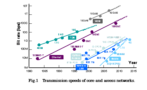
The further enhancement of TDM access technologies beyond ten gigabits is facing various barriers to cost-effective realization: the history of the core network has proven this. In addition, a higher-speed TDMA requires higher-rate burst-mode circuits. Given this, one of the most attractive candidates for future optical access next to 10G-EPON and 10G-PON is WDM-PON, in which each signal from/to each user occupies a different wavelength. WDM-PON is a physically shared system, but a logically unshared system. This provides certain advantages as follows.
Å@Å@Å@1. The bandwidth for each user can be easily upgraded.
Å@Å@Å@2. Various services can be provided per wavelength.
Å@From the viewpoint of advantage 2, integration/convergence with wired and wireless access will flexibly provide broadband services in next generation access networks. The recent progress of cloud computing needs a broadband wireless access easily connecting to high definition videos and rich Web applications with smart phones and tablet computers anywhere, at any time as shown in Fig. 2, so that one of the most important targets for next generation wireless access is to realize a higher throughput equivalent to current optical access. Recent proposals have aimed to provide current wireless and/or wired services over WDM-PON [5]-[8].
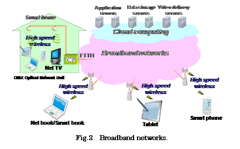
This report reviews the technical issues of WDM-PON, some solutions, and their applications to simultaneously achieve wired and wireless access on the same platform. Section 2 describes our focus on two candidate applications of WDM-PON: one is WDM-PON based on wavelength router for metro/access integration and green field, and the other is a short-reach WDM-PON co-existing with current PON systems. We identify that the realization of colorless optical network units (ONUs) is an important technical issue for both applications, and an effective protection function is another important issue, especially for the long-reach WDM-PON. Next, we review several Åecolorless-ONUÅf approaches as well as address several issues raised by some colorless ONU approaches. We also describe a long-reach WDM-PON architecture with a wavelength shifted protection scheme as well as loop back type colorless ONUs. In Section 3, we show a wide-area wired/wireless integrated access network based on long-reach WDM-PON architecture. Section 4 describes the other architecture to provide wired and wireless services based on a short-reach WDM-PON that coexists with a current PON system and broadband mobile backhaul.
2. Technical issues of WDM-PON
Figure 3 summarizes the application and technical issues for two options to implement WDM-PON: one is to use wavelength routers and the other is to use power splitters in the optical distribution networks (ODNs). The wavelength-router-based WDM-PON, where wavelength allocation is basically static, is applicable to short-reach access for green field (e.g. broadband mobile backhaul) and long-reach access due to the low loss-budgets of the wavelength routers. The power-splitter-based WDM-PON is applicable to migration scenarios from legacy PONs, since they use the same ODNs as the existing infrastructure. Here, dynamic wavelength allocation is possible [9], because the power splitters are transparent to wavelength. The researches of WDM-PON are mainly focused on two applications: one is a long-reach WDM-PON based on wavelength routing for metro/access integration, and the other is a short-reach WDM-PON for co-existence with current PON systems.
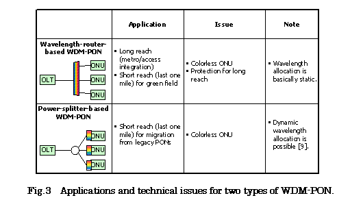
The common technical issue in both types of WDM-PON is the colorless ONU; the ONUs should be colorless (in other words, no ONU is wavelength specific) to reduce the costs of operation, administration, and maintenance (OA&M) functions, as well as the production cost, since mass production becomes possible with just one specification. Another issue, especially for the long-reach WDM-PON, is a protection function that can counter feeder fiber breaks. The rest of this section describes the various colorless-ONU techniques and the protection function for the long-reach WDM-PON.
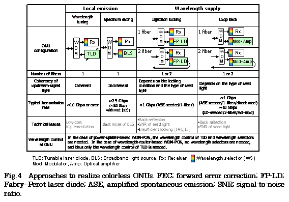
Many colorless proposals have been reported [10]-[18]. The proposals can be summarized into two main schemes as shown in Fig. 4: local emission and wavelength supply. In the case of the power-splitter-based WDM-PON, wavelength selectors (WSs) are needed. Note that no WSs are needed in the case of the wavelength-router-based WDM-PON, because the wavelength from/to each ONU is selected by the wavelength-router. We select the colorless ONU scheme suitable for the application shown in Fig.3. Enabling technologies for the two schemes are described in this section.
2.1. Local emission scheme
There are two local emission approaches: a wavelength tuning [10] and spectrum slicing [11], [12]. The ONU of the wavelength tuning approach consists of a tunable laser diode (TLD) as a transmitter (Tx), an optical receiver (Rx) with WS, and a WDM coupler that divides/combines the upstream and downstream signals. The wavelength-tunable scheme is expected to achieve a large loss budget and high speed operation at 10 Gbps, because a coherent light is used. To achieve Tx and Rx tunability with ease for WDM-PONs based on the power-splitter, a tunable fiber ring laser is another option, where the wavelength selector might be simultaneously used for selecting the downstream wavelength. We have reported the feasibility of the fiber ring laser using a semiconductor optical amplifier (SOA) and an optical tunable filter (OTF), which operated over a 20-nm wavelength range with accuracy of +/- 1.75 GHz [19].
The configuration of the ONU in the spectrum slicing approach is similar to that in the wavelength tuning approach except that a broadband light source (BLS) with WS is used instead of the TLD. The advantage of the spectrum slicing approach in wavelength-router-based WDM-PONs is its light sources, e.g. superluminescent diodes (SLDs) under quasi-athermal operation without precise wavelength control can be used. A particular noise factor in the spectrum slicing approach is the signal-signal beat noise. The signal-to-noise ratio (SNR) of the signal-signal beat noise can be expressed as being proportional to the ratio of the data rate to sliced bandwidth [12]. To realize high speed operation, broadening the sliced bandwidth is inevitable; it follows that the number of available channels decreases assuming the light source has a fixed bandwidth. Broadening the sliced bandwidth also increases the fiber dispersion penalty. The use of forward error correction (FEC) can effectively overcome this drawback. The 10-Gb/s, eight channel spectrum-sliced DWDM transmission with the channel spacing of 200 GHz was confirmed through the use of FEC [12].
2.2. Wavelength supply scheme
There are two approaches to wavelength supply scheme: injection locking [13]-[15] and loop back approach [16]-[18]. In the injection locking approach, the ONU consists of a Fabry-Perot laser diode (FP-LD) as the Tx, an Rx with WS, and a WDM coupler that divides/combines the upstream and downstream signals and/or the injection light. The spectrum sliced light or laser light is injected into the FP-LD, so as to lock the wavelength of the upstream signal. The relative intensity noise (RIN) of the upstream signal (injection locked light) depends on the injection locking condition [14], [15].
In the loop back approach, the ONU consists of an optical modulator (Mod) and optical amplifier (Amp) as the Tx, an Rx with WS, and a WDM coupler that divides/combines the upstream and downstream signals and/or continuous wave (CW) light. The CW light supplied from the OLT is modulated and amplified by the Mod and Amp, respectively, to generate the upstream signal.
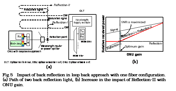
To avoid the degradation due to back reflection of the upstream signal, one option is to base wavelength supply on the two-fiber configuration; the long-reach WDM-PON described in Section 3 assumes this configuration. In the one-fiber configuration, two types of back reflection, the back reflection of continuous wave (CW) light from the OLT (reflection I) and that of the modulated signal from the ONU (reflection II), as shown in Fig. 5 (a), must be considered, because the interference between the signal and back reflection degrades the received SNR due to intensity noise [20]. The impact of reflection-II increases strongly with ONU gain, so that the received SNR falls as ONU gain is increased, as shown in Fig. 5 (b) [20]. To reduce the impact of reflection-II, we employ a gain-saturated SOA in the ONU [21].
2.3. Protection function
In the long-reach WDM-PON, the failure of the feeder fiber carrying the WDM signals may cause the loss of data for all users. Thus, a protection function for the feeder fiber is required to realize the reliable WDM-PON. Several approaches have been proposed to achieve the protection needed [22]-[24]; they use 3-dB optical couplers to split (or combine) the path of WDM signals to/from both the working and protection fibers in the OLT or in the wavelength router. Note that the OLT and the wavelength router are typically located in the central office (CO) and in the access node (AN), respectively. This protection scheme, unfortunately, has a low loss budget, because of the use of the 3-dB optical couplers [22]-[24]. To address this issue, we have proposed and demonstrated a wavelength-shifted protection scheme utilizing the cyclic property of the 2Å~N athermal arrayed-waveguide grating (AWG) and two wavelength allocations, one each for working and protection, which does not use 3-dB optical couplers for protection [25]. While this protection scheme can be applied to WDM-PONs with various types of colorless ONU, the loop-back approach is the most suitable choice because we do not need any protection function in the ONUs.
3. Long-reach WDM-PON
3.1 Wide-area wired/wireless integrated access network
The growth of e-businesses is accelerating strong demands for broadband services over gigabit, for business users. Such business users need wide-area broadband access networks that offer high-speed connection services between several local area networks [16]. The long-reach WDM-PON promises a wide-area access network that realizes consolidated operation to reduce OA&M cost, because it can offer from gigabit to ten gigabit-class guaranteed-bandwidth services according to user demand.
Figure 6 illustrates the wide-area wired/wireless integrated access network based on long-reach WDM-PON [26]. OLTs and an optical carrier supply module (OCSM) are located in the center node; the OCSM is an optical frequency comb generator that supplies multi-wavelength carriers to several OLTs. The OLT has interfaces for radio-on-fiber access (RoF IFs) as well as those for high speed optical access such as 10 Gigabit Ethernet (10GE IFs). The RoF approach simplifies the system architecture by directly delivering broadband signals of radio frequency through optical fibers.
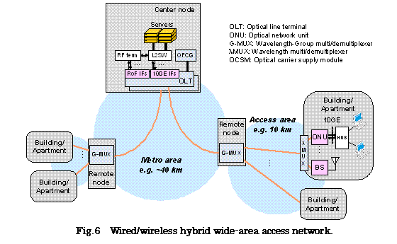
One of the most attractive RoF approaches over 100Mbps with the millimeter band is to heterodyne two optical frequencies whose difference corresponds to the radio frequency (RF), e.g. 60 GHz [27]. By modulating one of two optical frequencies before fiber transmission, the RF signal can be extracted by heterodyne detection after fiber transmission. This approach can eliminate not only the local RF generator in each base station (BS), but also achieve better fiber-transmission performance than sub-carrier modulation (SCM) approach due to the fiber dispersion. However, the two optical frequencies must be precisely controlled to generate a stable RF signal after detection. The OCSM that can inherently provide such precise frequency control between any two wavelengths are an attractive candidate for this purpose as well as for multiplexing many different RF signals.
Å@This network uses DWDM wavelength channels (e.g. 64 channels) and the group multi/demultiplexer (G-MUX) in each remote node divides/combines the DWDM channels into/from several groups of wavelengths (e.g. 8 wavelengths x 8 groups). Each wavelength group is dedicated to a building/apartment, where a wavelength pair can provide either optical access via an ONU or RoF access with a BS (e.g. 1 x 10GE-ONU and 3 x RoF BSs in each building/apartment).
3.2. System Configuration of wide-area wired/wireless integrated access network
Figures 7 (a) and (b) show the configuration and optical spectrum of the OCSM that we reported previously [28]. By modulating the CW lights of seed laser diodes (LDs λ1 to λn in the figure) with a phase modulator (PM) and an intensity modulator (IM) using 25-GHz radio frequencies with appropriate amplitudes, we can obtain multi-wavelength optical carriers as the modulation sideband as shown in Fig. 7 (b); the spectrum consists of four wavelength groups where each group consists of eight wavelengths with 25-GHz spacing. Typically, low-cost optical filters for group multi/demultiplexing require an adequate guard-band between neighboring groups. As shown in the spectrum, this OCSM is very suitable for such a group multi/demultiplexing because one can easily adjust the spacing between neighboring wavelength groups by adjusting the seed wavelengths.
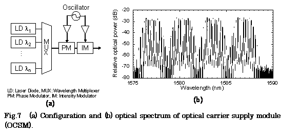
Figure 8 shows a detailed configuration of the proposed network system. Wavelength pairs to be used for an ONU or a BS are λk1/λk3, λk2/λk4, λk5/λk7, λk6/λk8 where k is the group number (k = 1 Å` n). In the case of the OCSM shown in Fig. 7 (b), n is 4; we can increase n by adding seed wavelengths to OCSM. The center node consists of n sets of modulation arrays (Mod array), n sets of receiver arrays (Rec array) and group multi/demultiplexers (G-MUX/G-DMX). Each Mod array multi/demultiplexes the eight wavelengths in each group by using arrayed-waveguide gratings (AWGs), and λk1, λk2, λk5, λk6 are modulated by 10Gbit/s binary NRZ data (for optical access) or 10GHz-band IF data (for RoF access). In the remote node, the G-MUX/DMX divides/combines signals by wavelength groups. In the building, AWGs multi/demultiplex the eight wavelengths. The BS receives the RoF signal by heterodyning the wavelength pair (e.g. λk1/λk3) to generate a wireless signal with 60-GHz RF as well as transmitting the RoF signal by remotely modulating and transmitting one of the wavelength pairs (e.g. λk3) upstream [29]. The ONU simply receives one modulated wavelength pair (e.g. λk2) as well as modulating/demodulating another wavelength pair (e.g. λk4). Figure 9 summaries the signal spectra of OLT, ONU, and OLT. By using this system configuration, we can realize a wide-area access network that provides both high-speed optical access and fiber-wireless access flexibly depending on need.
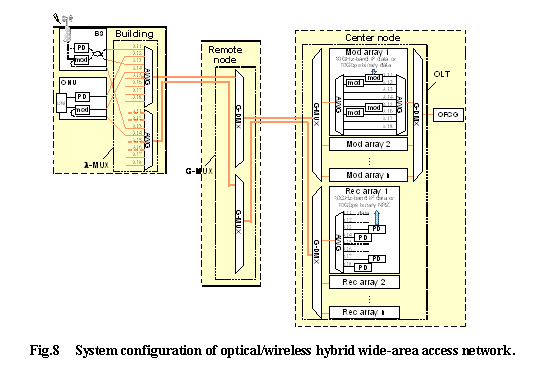
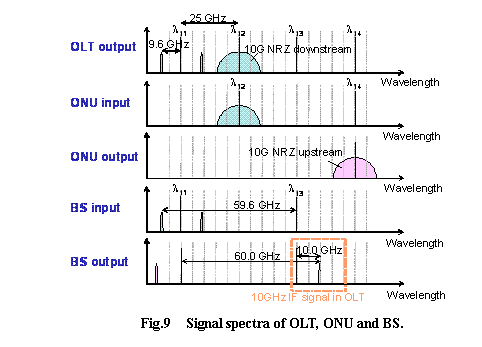
4. Short-reach WDM-PON
4.1. Co-existence with current PON system
Figure 10 illustrates the migration to WDM-PON, that accommodates wired and wireless services, from the current PON system via the common power-splitter-based ODN. The WDM-OLT and the WDM-ONU in Fig. 10 for WDM-PON can be simply added without changing the ODN: the WDM-OLT comprises multiple optical subscriber units (OSU), each of which communicates with a WDM-ONU. The detailed wavelength allocation is also shown in Fig. 10. According to the standardization bodies, the upstream and downstream wavelengths of the current PON systems range from 1260 to 1360 nm and from 1480 to 1500 nm, respectively. The wavelengths for video use lie in the range of 1550 to 1560 nm. The simplest approach to wavelength allocation for WDM-PON is to use the L band, which is located in the wavelength region that is longer than that reserved for video use. On the assumption that many wavelengths will be needed to accommodate a large number of users, DWDM technologies will play an important role in efficiently utilizing the limited wavelength region available.
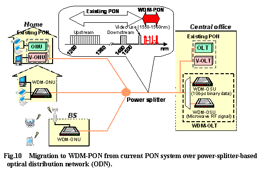
To construct an easy to use power-splitter-based WDM-PON for mass users, plug-and-play functionality is essential [10]. Plug-and-play means automatic wavelength control of the ONU, which is as critical as the precise time control needed in the current PON based on TDMA.
We demonstrated wavelength-tuning colorless ONUs with the plug-and play function [10], from the viewpoint of realizing the transmitter without WS. Wavelength control can be achieved with initial wavelength setting and wavelength stabilization. The former remotely and automatically establishes the initial wavelengths between each ONU and the OLT. After the initial wavelength is set, wavelength stabilization is carried out. This is especially critical if the channel spacing is narrow, and thus the multi-wavelength monitoring technique [30] is required.
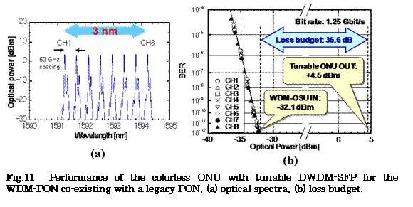
Figs. 11 (a) and (b) show the optical spectra and loss budget of the colorless ONU based on a SFP (Small Form-Factor Pluggable) for the WDM-PON that can co-exist with a legacy PON [31]. The DFB-LDs in SFPs are directly modulated with 1.25Gbps binary data. The 3-nm tunable range, which provides 8 channels with 50 GHz spacing, was verified in [29]: wavelength tuning was realized via temperature control of the laser in the SFP. The loss budget between the WDM-OSU and colorless ONU (WDM-ONU in Fig. 10) was reported in [30] as over 36 dB, which is sufficient to support the adoption of legacy ODNs. To provide wireless services with microwave band simultaneously over the WDM-PON, digitized RoF techniques [32] are available to directly modulate the DFB-LD in SFP with digitized RF signals.
4.2. Broadband mobile backhaul
Because of the strict limitation imposed by the radio frequency spectrum, the increase of the wireless access throughput needs to the reduction of cell size, and thus wired access networks accommodate a huge number of base stations (BSs) to cover a wide area. The femto-cell architecture provided by broadband optical access network is a promising approach to realize the next generation broadband wireless access. We have proposed the radio over fiber (RoF) distributed antenna system (DAS) over WDM-PON architecture [33] to combine WDM access [1] and a DAS with multiple input multiple output (MIMO) technologies [34], as shown in Fig. 12. The provision of various wireless services per wavelength in WDM-PON can be accommodated with RoF-DAS technologies. This technical convergence will achieve the universality for various types of broadband air-interfaces expected to the Gbps class throughput, the flexibility for non-uniform traffic distribution, and the user-mobility in wireless service area.
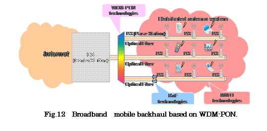
Figure 13 illustrates a configuration of WDM-PON, where two wavelengths are assigned to each BS as an up- and down-stream. We employ a 2 x N arrayed waveguide gratings (AWGs) as a wavelength multi/demultiplexer, to achieve a low dissipation for accommodating a large number of BSs in single feeder fibers. At the CS, four MIMO RF signals for different four cells are multiplexed in the MIMO signal processing in Fig. 12. Each BS consists of an optical circulator without any wavelength selectivity to make it easy to add upstream signals and drop downstream signals. Optical filters, such as fiber gratings, at the BS are used to select a wavelength assigned to the BS. This configuration achieves the transparency of transmission lines through its lack of optical filters, and thus has scalability of upgrading wavelength channels in the future. To decrease the costs of operation, administration, and maintenance functions, as well as the production cost, we can introduce wavelength tunability in LDs and fiber gratings of BSs; that is colorless BS.
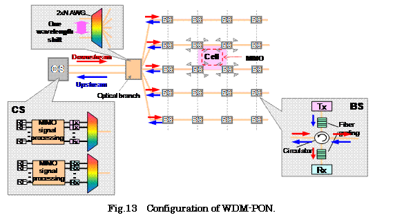
At the CS and BSs, four MIMO RF signals can be multi/demultiplexed over a wavelength, and transmitted by using subcarrier-multiplexing (SCM) technique. As for the multiplexing techniques of four MIMO RF signals, we can employ frequency division multiplexing (FDM), time division multiplexing (TDM), or code division multiplexing (CDM). Since the FDM needs the frequency conversions of MIMO RF signals at CS and BS, the transparence of radio air-interfaces is diminished. Thus, the TDM or CDM is suitable to multiplex the MIMO RF signals. As compared with the TDM, CDM is complicated, and the sampling rate is higher than that of TDM. By using TDM, each MIMO RF signal is simply bandpass-sampled [35] and multiplexed with time domain, so as to achieve the transparency for different types of broadband radio air-interfaces. In addition, the TDM can easily extend to digitized RoF approach with the use of analog/digital and digital/analog converter, which mitigates the requirement for linear device characteristics of optical components [32].
Å@Figure 14 shows our experimental setup to transmit downstream signals of RoF-DAS over WDM-PON with optical TDM and the signal transition diagram at each component. We assumed that 2 x 2 MIMO signal transmission in a cell. Two wavelengths were used to realize 2 x 2 MIMO signal transmission; two 802.11n RF signals in the 2.4 and 5 GHz bands were multiplexed in each wavelength with optical TDM and transmitted to the BS.
Å@The two continuous lightwaves emitted from DFB-LDs were wavelength-multiplexed in Fig. 13 (a), and modulated with a lithium niobate Mach-Zehnder modulator (LN-MZM) driven with a return to zero (RZ) pulse of 100 ps pulse width at a 1 GHz repetition rate from a pulse pattern generator (PPG) in Fig. 13 (b). Two wavelength signals were amplified with an erbium doped fiber amplifier (EDFA) and demultiplexed with an AWG of 25 GHz wavelength spacing. Each wavelength was divided with a 3 dB coupler and modulated with each LN-MZM driven by 802.11n RF signals with 40 MHz bandwidth whose center frequencies were 2.422 GHz (ch 3) and 5.230 GHz (ch 46) from the vector signal generator (VSG) in Fig. 13 (c). At the output of each LN-MZM, we obtained the bandpass-sampled RF signals of the 2.4 and 5 GHz bands. The modulation and coding scheme (MCS) index of 802.11n RF signals was 15 [36] i.e. 64-quadrature amplitude modulation (QAM) orthogonal frequency division multiplexing (OFDM) signals. We employed optical delay lines and 3 dB couplers to optically multiplex the bandpass-sampled RF signals and dummy RF signals of an adjacent cell, as shown in Fig. 13 (d). The optically multiplexed RF signals were wavelength-multiplexed again and transmitted through the optical feeder fiber as a downstream signal.
Å@The transmitted signals from the CS were distributed to each BS with the AWG, and the wavelength assigned at the BS was dropped by the 3-port circulator. The downstream signal dropped at the BS was converted by the photo diode transimpedance amplifier (PD-TIA), and demultiplexed with a high-speed electrical switch (SW) in Fig. 13 (f). The SW was driven by a control signal with a 300 ps pulse width at 1 GHz repetition rate from the PPG. The demultiplexed RF signals were converted to original RF signals with the band pass filter (BPF), which were transmitted as wireless signals from antennas at BS in Fig. 13 (g).
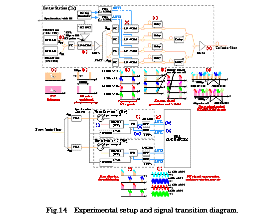
Figures 15 (a) and (b) show the analyzed RF signals of λD1 and λD2, respectively. The EVM values of -22.7 and -21.9 dB were obtained, respectively. The optical powers at the PD-TIA input and the electrical powers at the VSG output were the same values without the multipath fading. Figure 14 (c) and (d) depict the the RF spectrum of of λD1 and λD2. The experimental results confirm the basic feasibility of optical TDM and bandpass-sampled MIMO RF signal transmission in the proposed RoF-DAS over WDM-PON architecture.
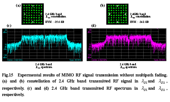
5. Summary
We have described the technical issues, solutions, and applications of WDM-PON. The WDM-PON can construct scalable and flexible networks to provide wired and/or wireless services, so it is the leading candidate for the next generation optical access systems beyond 10 Gbps TDMA systems. The main technical issue of WDM-PON was how to realize the colorless ONU. Two candidates, local emission and wavelength supply, were summarized and their features were explained in detail. The requirements and technical issues related to the protection function for the feeder fibers of WDM-PON were elucidated. We described the applications of long- and short-reach WDM-PON. The former offers wide-area wired/wireless integrated access networks that can accommodate the large number of business users expected. The latter enables migration from the current PON systems by utilizing the current infrastructure. The requirements and technical issues associated with the plug-and-play function, which remotely and automatically establishes the initial wavelengths of each ONU, were discussed. The wireless services can be also accommodated with the short-reach WDM-PON utilizing the microwave band RoF techniques. We also mentioned broadband mobile backhaul utilizing short-reach WDM-PON based on wavelength router. The radio over fiber (RoF) distributed antenna system (DAS) over WDM-PON architecture was proposed to combine WDM access and a DAS with multiple input multiple output (MIMO) technologies. The preliminary experiments were demonstrated to confirm the feasibility of the proposed network architecture.
[2] Broadband Passive Optical Networks, ITU-T Recommendation G.983.3.
[3] http://www.ieee802.org/3/av/
[4] http://www.fsanweb.org/ngpon.asp
[5] K. Tsukamoto, T. Nishiumi, T. Yamagami, T. Higashino, S. Komaki, R. Kubo, T. Taniguchi, J. Kani, N. Yoshimoto, H. Kimura, and K. Iwatsuki, ÅgConvergence of WDM Access and Ubiquitous Antenna Architecture for Broadband Wireless ServicesÅh, Progress In Electromagnetics Research Symposium (PIERS) 2010.
[6] K. Prince, J. B. Jensen, A. Caballero, X. Yu, T. B. Gibbon, D. Zibar, N. Guerrero, A. V. Osadchiy, and I. T. Monroy, ÅgConverged Wireline and Wireless Access Over a 78-km Deployed Fiber Long-Reach WDM PONÅh, IEEE Photonics Technol. Lett., Vol.21, No.17, pp.1274-1276 (2009)
[7] W-T. Shaw, S-W. Wong, S-H. Yen, and L. G. Kazovsky, ÅgAn Ultra-Scalable Broadband Architecture for Municipal Hybrid Wireless Access Using Optical Grid NetworkÅh, Optical Fiber Communication Conference and Exposition and National Fiber Optic Engineers Conference (OFC/NFOEC), 2009, OThP2.
[8] Z. Jia, J. Yu, G. Ellinas, G. K. Chang, "Key enabling technologies for optical-wireless networks: optical millimeter-wave generation, wavelength reuse, and architecture,", IEEE J. Lightwave Technol., Vol.25, No.11, pp.3452-3471, (2007).
[9] F. T. An, K. S. Kim, D. Gutierrez, S. Yam, E. Hu, K. Shrikhande, L. G. Kazovsky, ÅgSUCCESS: a next-generation hybrid WDM/TDM optical access network architecture,Åh, IEEE J. Lightwave Technol., Vol.22, No.11, pp.2557 - 2569 (2004).
[10] H. Suzuki, M. Fujiwara, T. Suzuki, N. Yoshimoto, K. Iwatsuki, and T. Imai, ÅgColorless and plug & play technologies for WDM access over existing power-splitter-based infrastructureÅh, J. Optical Networking Vol.6, No.7, pp. 830-839 (2007).
[11] K. Akimoto, J. Kani, M. Teshima, and K. Iwatsuki, ÅgGigabit WDM-PON system using spectrum-slicing technologies,Åh in Proceedings of the 29th European Conference on Optical Communication (ECOC2003) (IEEE, 2003), paper Th2.4.6.
[12] S. Kaneko, J. Kani, K. Iwatsuki, A. Ohki, M. Sugo, and S. Kamei, ÅgScalability of spectrum sliced DWDM transmission and its expansion using forward error correction,Åh J. Lightwave Technol. 24, 1295-1301 (2006).
[13] H. D. Kim and C.-H. Lee, ÅgWavelength-division multiplexed passive optical network using Fabry-perot laser diodes,Åh in Proceedings of the Optoelectronics and Communications Conference (OECC2002) (IEICE, 2002), paper 10P-15.
[14] M. Fujiwara, H. Suzuki, K. Iwatsuki, and M. Sugo, ÅgNoise characteristics of signal reflected from ASE-injected FP-LD in loopback access networksÅh, Electron.Lett., Vol.42, No.2, pp.111-112 (2006).
[15] K. Y. Park, C. H. Lee, ÅgNoise Characteristics of a Wavelength-Locked Fabry-Perot Laser Diode,Åh IEEE J. Quantum Electron., Vol.44, No.11, pp. 995-1002 (2008).
[16] J. Kani, M. Teshima, K. Akimoto, N. Takachio, H. Suzuki, K. Iwatsuki, and M. Ishii, ÅgA WDM-based optical access network for wide-area gigabit access services,Åh IEEE Commun.Mag. 41, S43-S48 (2003).
[17] F. Payoux, P. Chanclou, and R. Brenot, ÅgWDM PON with a single SLED seeding colorless RSOA-based OLT and ONUs,Åh presented at the European Conference on Optical Communication, Cannes, France, 24-28 September 2006, paper Tu4.5.1.
[18] J. M. Oh, S. G. Koo, D. Lee, S. J. Park, ÅgEnhancement of the Performance of a Reflective SOA-Based Hybrid WDM/TDM PON System With a Remotely Pumped Erbium-Doped Fiber Amplifier,Åh IEEE J. Lightwave Technol., Vol. 26, No.1, pp.144 - 149 (2008).
[19] J. Kani, and K. Iwatsuki, ÅgA wavelength-tunable optical transmitter using semiconductor optical amplifiers and an optical tunable filter for metro/access DWDM applicationsÅh, IEEE J. Lightwave Technol., Vol.23, No.3, pp.1164-1169 (2005).
[20] M. Fujiwara, J. Kani, H. Suzuki, and K. Iwatsuki, ÅgImpact of backreflection on upstream transmission in WDM single-fiber loop back access networksÅh, IEEE J. Lightwave Technol., vol.24, No.2, pp.786-796 (2006).
[21] M. Fujiwara, H. Suzuki, N. Yoshimoto, and K. Iwatsuki, ÅgLoss budget expansion technique using gain-saturated SOA in WDM single-fiber loopback access networksÅh, Opt. Fiber Technol. Vol.13, No.1, pp.72-77 (2007).
[22] S. B. Park, D. K. Jung, D. J. Shin, H. S. Shin, S. H. Hwang, Y. J. Oh, and C. S. Shim, ÅgBidirectional wavelength-division-multiplexing self-healing passive optical network,Åh presented at the Optical Fiber Communication (OFC), Anaheim, CA, 2005, Paper JWA57.
[23] T. J. Chan, C. K. Chan, L. K. Chen, and F. Tong, ÅgA self-protected architecture for wavelength-division-multiplexing passive optical networksÅh, IEEE Photon. Technol. Lett., vol. 15, no. 11, pp. 1660-1662 (2003).
[24] E. S. Son, K. H. Han, J. H. Lee, and Y. C. Chung, ÅgSurvivable network architectures for WDMPON,Åh Optical Fiber Communication (OFC), 2005, Paper OFI4.
[25] H. Nakamura, H. Suzuki, J. Kani, and K. Iwatsuki, ÅgReliable Wide-Area Wavelength Division Multiplexing Passive Optical Network Accommodating Gigabit Ethernet and 10 Gigabit Ethernet ServicesÅh, IEEE J. Lightwave Technol., Vol.24, No.5, pp.2045-2051 (2006).
[26] Junichi Kani, ÅgTrends in next generation optical access networks and a proposed hybrid optical/wireless wide-area access networkÅh, Progress In Electromagnetics Research Symposium (PIERS) 2008, pp.421-425 (2008)
[27] T. Taniguchi, N. Sakurai, K. Kumozaki, and T. Imai, ÅgLoop-back Optical Heterodyne Technique for 1.0-Gb/s Data Transmission Over 60-GHz Radio-On-Fiber Uplink,Åh IEEE J. Lightwave Technol., vol. 25, pp.1484-1494 (2007).
[28] M. Fujiwara, M. Teshima, J. Kani, H. Suzuki, N. Takachio, and K. Iwatsuki, ÅgOptical carrier supply module using flattened optical multicarrier generation based on sinusoidal amplitude and phase hybrid modulationÅh, IEEE. J. Lightwave Technol., Vol.21, No.11, pp.2705-2714 (2003).
[29] T. Sono, Y. Takahashi, T. Nakasyotani, H. Toda, T. Kuri, and Ken-ich Kitayama ÅgFull-Duplex 25-GHz Spacing DWDM MM-Wave-Band Radio-on-Fiber System Using a Supercontinuum Light Source and Arrayed-Waveguide-Grating FiltersÅh, Tech. Dig. of International Topical Meeting on Microwave Photonics (MWP) 2006.
[30] M. Fujiwara, H. Suzuki, K. Iwatsuki, T. Imai and, ÅgMultiwavelength monitoring by dithering temperature of directly-modulated laser diodesÅh, Electron.Lett., vol.42, No.13, pp.770-771 (2006).
[31] H. Suzuki, M. Fujiwara, T. Suzuki, N. Yoshimoto, H. Kimura, and M. Tsubokawa, ÅgWavelength-tunable DWDM-SFP transceiver with a signal monitoring interface and its application to coexistence-type colorless WDM-PON,Åh in Proceedings of the 33rd European Conference and Exhibition of Optical Communication (ECOC2007), Post-deadline paper PD3.4.
[32] A. Nirmalathas, P. A. Gamage, C. Lim, D. Novak, R. Waterhouse, and Y. Yang, ÅgDigitized RF transmission over fibersÅh, IEEE Microwave Magazine, June, pp.75-81, (2009).
[33] K. Tsukamoto, T. Nishiumi, T. Yamakami, T. Higashino, S. Komaki, R. Kubo, T. Taniguchi, J. Kani, N. Yoshimoto, H. Kimura, and K. Iwatsuki, ÅgConvergence of WDM access and ubiquitous antenna architecture for broadband wireless servicesÅh, PIERSÅ@Online, Vol. 6, No. 4, pp.385-389 (2010).
[34] S. Okamura, M. Okada, K. Tsukamoto, S. Komaki, H. Yamamoto, ''Impact of successive interference canceller on the performance of ubiquitous antenna-based SDMA system'', Electronics and Communications in Japan, Part 3 (Fundamental Electronic Science), 1, no.3, pp.10-24 (December 2004).
[35] R. G. Vaughan, N. L. Scott, and D. R. White, ÅgThe Theory of Bandpass SamplingÅh, IEEE Trans. on Signal Processing, Vol.39, No.9 pp.1973-1984 (1991).
[36] IEEE Std 802.11n-2009.
D11. Body Area Network
Y. Kado
Kyoto Institute of Technology
TThe advancement in sensing, embedded computing, and wireless communication has accelerated the progress of adopting sensor networks to form Wireless Body Area Networks (BAN or WBAN). BAN integrates wireless sensors, RFID tags, and other pervasive devices within and around human bodies for constructing diverse and practical systems for human computer interaction, physiological monitoring, and provision of entertainment. In the past few years, much of the research in the area of BAN has focused on challenges related to channel model, reliability, flexible network architectures, wearable transceiver designs, lightweight security solutions, and lifestyle applications.
Å@An important step in the development of BAN is the characterization of the electromagnetic wave propagation from devices that are close to or inside the human body. As the antennas for BAN applications are placed on or inside the body, the BAN channel model needs to take into account the influence of the body on the radio propagation. The IEEE 802.15.6 Task Group is developing a communication standard optimized for low power devices and operation on, in or around the human body to serve a variety of applications [1]. To develop more detailed models, the static path loss and impulse response models for BAN were also reported [2].
The human body is not an ideal medium for radio frequency wave transmission. It is partially conductive and consists of materials of different dielectric constants, thickness, and characteristic impedance. Therefore depending on the frequency of operation, the human body can lead to high losses caused by power absorption, central frequency shift, and radiation pattern destruction [1]. The absorption effects vary in magnitude with both frequency of applied field and the characteristics of the tissue. This makes it difficult to drive a simple path loss model for BAN and design antennas of wearable transceivers.
Å@One of the most promising approach to avoid this problem is a near-body quasi-static electric-field communication system that uses the surface of the human body as a data transmission path [3], [4], [5], [6]. A key aspect of the technology is the behavior of an alternating current (AC) electric field, which can be summarized in terms of three components produced around the body when an AC signal is applied to a parallel-plate electrode attached to the body. These components, which are all related to distance r from the body, are: the quasi-static electric field (proportional to 1/r3), the induced electric field (proportional to 1/r2), and the emitted electric field (proportional to 1/r). The near-body electric-field communications technology uses the quasi-static electric field, which attenuates steeply with r [6].
Å@As shown in Figures 1 and 2, the system consists of a transmitter that emits an AC electric-field signal modulated by input data from an electrode and a receiver that uses another electrode to read the weak AC electric field on the body induced by the signal and demodulates it to recover the data from it. The electronic devices in contact or in close proximity to the human body can use its conductive properties to establish body coupled communication between each other. This human centric communication paradigm can be used for BAN to reduce the impact of interference on/from RF systems, to avoid the fading effect that the body has on radio systems and to enable power efficient wireless links.
Å@To suppress electromagnetic radiation, NTT adopted a baseband transmission system with a newly developed electrooptic (EO) sensor in which the quasi-static electric field is directly modulated by 10 BASE-T data signal. They succeeded in 10-Mb/s data transmission through the human body and discussed the advantages of using the EO sensor for intrabody communication [7], [8], [9]. For this technology to come into wide personal use, the transceiver module must be compact and inexpensive, so the electronic components should be fabricated as LSI chips. NTT has developed a small and low cost multi-chip module for miniaturization of communication device [10], [11]. The communication quality of the prototype terminals implementing them was evaluated [12], [13].
Å@The body coupled communication implementations using a wideband correlation-based transceiver [14], an inductive coupling transceiver [15], and a scalable double-FSK modulation transceiver have been successively reported. The main applied field of these transceivers is wearable body sensor network.
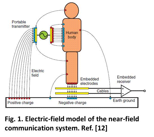
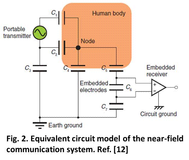
References
[2] J. Takada, T. Aoyagi et al., Åg Static Propagation and Channel Models in Body Area,Åh COST 2100 TD(08)639, Lille, France, 6-8 oct, 2008.
[3] T. G. Zimmerman, ÅgPersonal Area Networks: Near-field intra-body communication,Åh IBM Systems Journal, Vol. 35, Nos. 3&4, pp. 609-617, 1996.
[4] M. Shinagawa, M. Fukumoto, K. Ochiai, and H. Kyuragi, ÅgA near-field-sensing transceiver foy intrabody communication based on the electrooptic effect,Åh IEEE Trans. Instrum. Meas., Vol. 53, No. 6, pp. 1533-1538, 2004.
[5] Y. Kado, ÅgHuman-Area Networking Technology as a Universal Interface,Åh 2009 Symposium on VLSI Circuits Digest of Technical Papers, pp. 102-105, 2009.
[6] Y. Kado and M. shinagawa, "AC Electric Field Communication for Human-Area Networking,Åh IEICE Transactions on Electronics, Vol. E93-C, No. 3, pp. 234-243, 2010.
[7] A. Sasaki, A. Furuya, and M. Shinagawa, ÅgStudy of semiconductor electro- optic modulators for sensing extremely-low-frequency electrical signalsÅh, Sensors and Actuators A, vol. 151, no. 1, pp. 1-8, 2009.
[8] A. Sasaki, M. Shinagawa, and K. Ochiai, ÅgPrinciples and demonstration of intrabody communication with a sensitive electrooptic sensorÅh, IEEE Trans. Instrum. Meas., vol. 58, no. 2, pp. 457-466, 2009.
[9] A. Sasaki, A. Furuya, and M. Shinagawa, Åg10-Mbps short-range baseband wireless communications via quasi-static electric fieldsÅh, IEICE Trans. Commun., vol. E93-B, no. 1, 2010.
[10] Y. Kado and M. Shinagawa, ÅgRedTacton Near-body Electric-field Communications Technology and Its ApplicationsÅh, NTT Technical Review, Vol. 8, No. 3, Mar. 2010.
[11] R. Kawano, F. Morisawa, M. Shinagawa, and Y. Kado, ÅgLSIs for an Advanced Compact Electric-field Communication ModuleÅh, NTT Technical Review, Vol. 8, No. 3, Mar. 2010.
[12] A. Sasaki, R. Kawano, T. Ishihara, and M. Shinagawa, ÅgModeling of Human-body Near-field Communication and Evaluation of Communication QualityÅh, NTT Technical Review, Vol. 8, No. 3, Mar. 2010.
[13] T. Minotani and M. Shinagawa, 2010, ÅgHighly Efficient Signal-Inducing Transceiver and Evaluation over Human BodyÅh, AP-RASC'10, Toyama, BCK-1, 2010.
[14] A. Fazzi, S. Ouzounov, and J. Homberg,Åh A 2.75mW Wideband Correlation-Based Transceiver for Body-Coupled Communication,Åh Dig. Tech. Papers of 2009 IEEE International Solid-State Circuits Conference, pp. 204-205, Feb. 2009.
[15] S. Lee, J. Yoo, H. Kim, and H.-J. Yoo, ÅgA Dynamic Real-time Capacitor Compensated Inductive Coupling Transceiver for Wearable Body Sensor Network,Åh 2009 Symposium on VLSI Circuits Digest of Technical Papers, pp. 42-43, 2009.